Creating a double sided PCB with solder mask
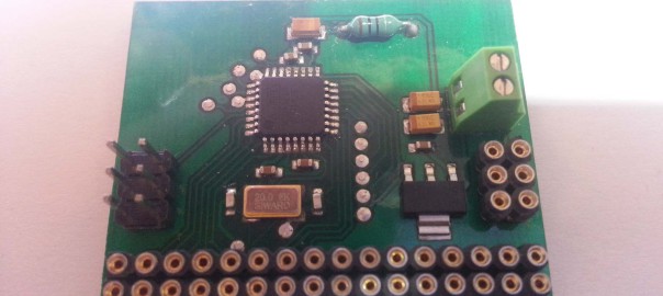
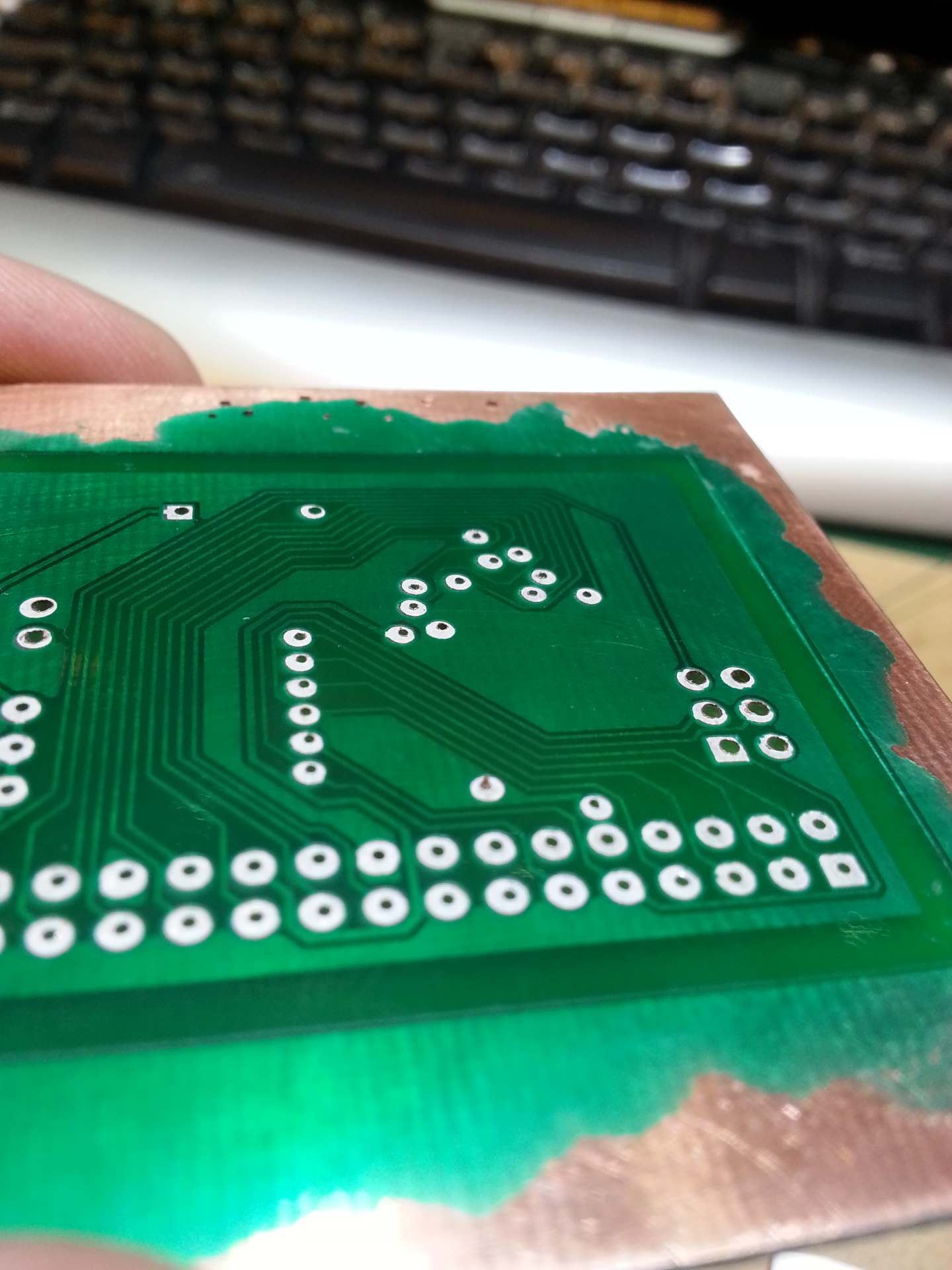
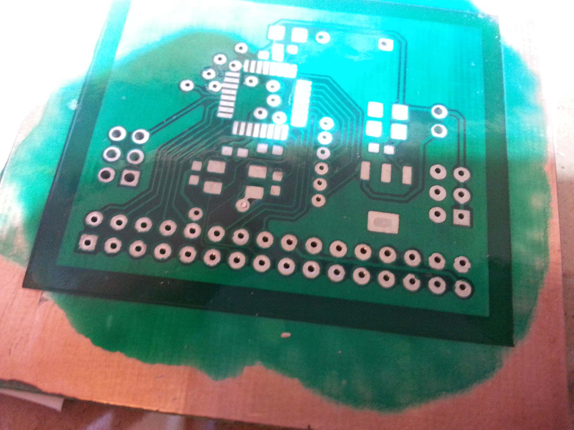
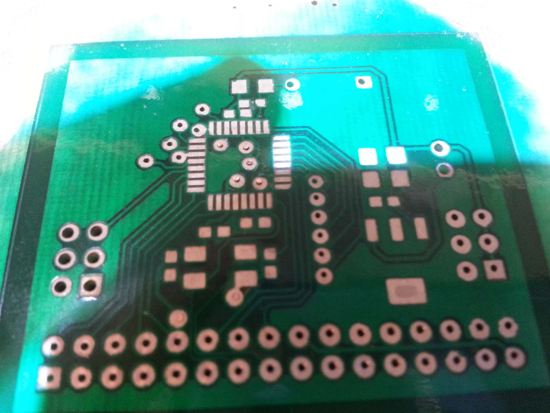
The PCB I create in this guide is a tiny breakout board for the ATmega88/ATmega168/ATmega328 series of microcontroller. It holds the MCU plus a 20MHz crystal, a voltage regulator, an ISP socket, a power socket, and a signal socket that expose all IO lines from the MCU. Very useful when prototyping with one of those MCUs before making a dedicated PCB.
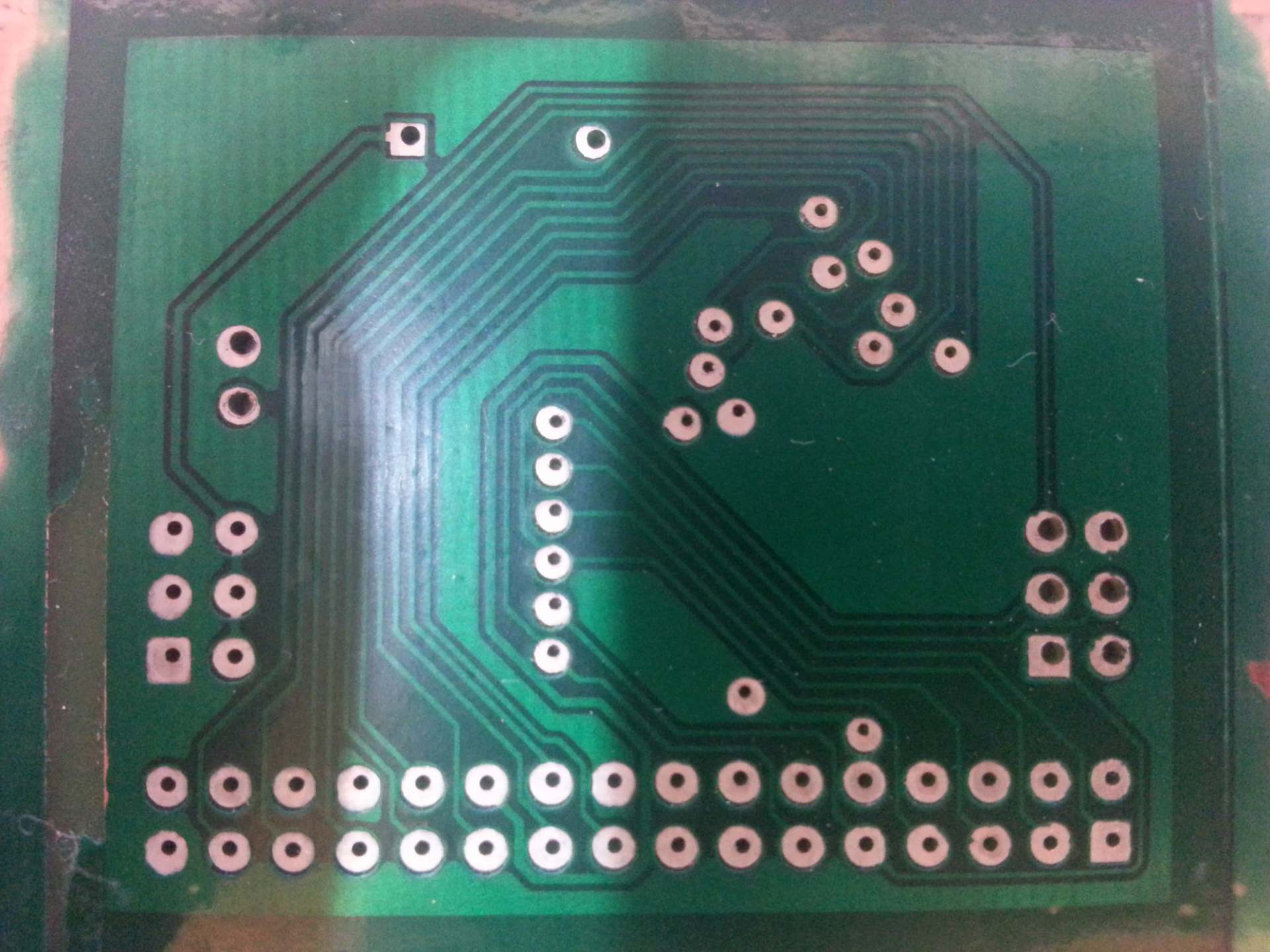
Most of the signal traces on the PCB is 10-mil, and most of the power traces are 15mil. And most of the spacing is 8-mil or more. There is however a small section where 6-mil traces with 5-mil spacing is used successfully. I partly did this to be able to fit 2 traces between the pins of one of the connectors, but mostly to see if my DIY skills and equipment where up to it 🙂 I try to not go smaller than 8-mil unless absolutely needed. 8-mil and up seems to give plenty of headroom, but 6-mil might not give a 100% yield. Although it has done so far. But then again, I have only made 1 attempt.
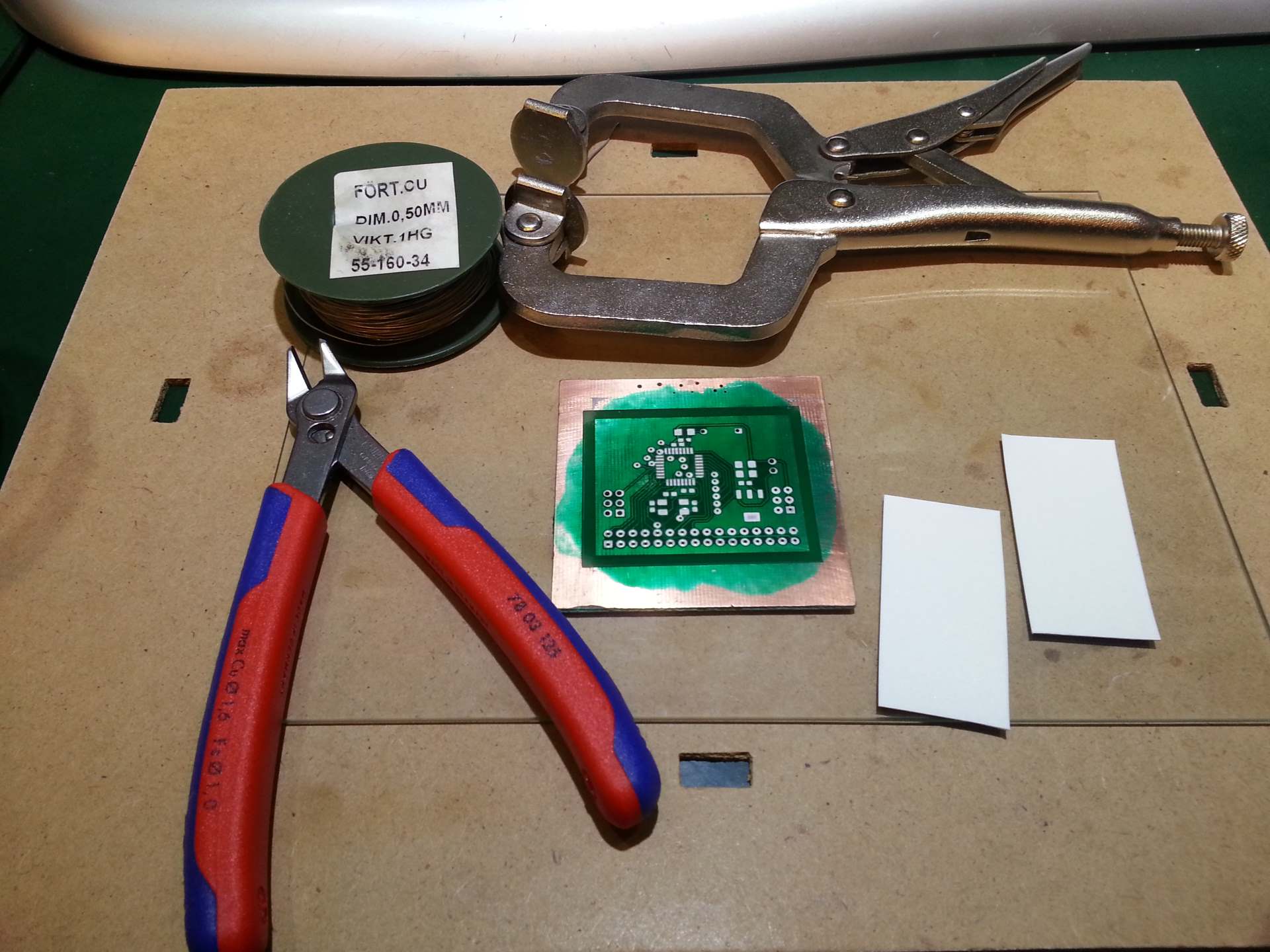
I use a few special tools in this guide. Mostly home made. And they do make the process quicker and easier. But don’t despair if you don’t have them. In most cases the result will be just as good without them, it will only be a bit more time consuming. The most notable tools I use are:
- UV exposure unit with a built in vacuum system.
- Heated and agitated etch tank.
- A camera guided drill jig.
- A light box.
- A modified laminator.
- Some “in house” python scripts for mask bitmap processing.
The post processing python scripts are not “consumer ready” 🙂 I will try to make them a bit more user friendly and add them here for download at some point. If you would like to have them before I get around to this, send me a mail at kavionicadm@gmail.com and I will try to get them to you.
Please try anything you see me do at home. I’m certainly not a trained professional. But be careful! Plenty of stuff down this list that can severely hurt you, or even kill you. I take no responsibility if your tongue get stuck in a hot-roll laminator, your arm is eaten by NaOH, or you get electrocuted by some faulty DIY equipment. Or any other unpleasant things that might happen from following these instructions. Don’t lick the laminator and use appropriate caution and protective gear, and you should be fine though.
Exporting UV masks (DipTrace specific)
This section is very specific to DipTrace which is my schematics capture and PCB layout package of choice. The general rules should apply to anything though.

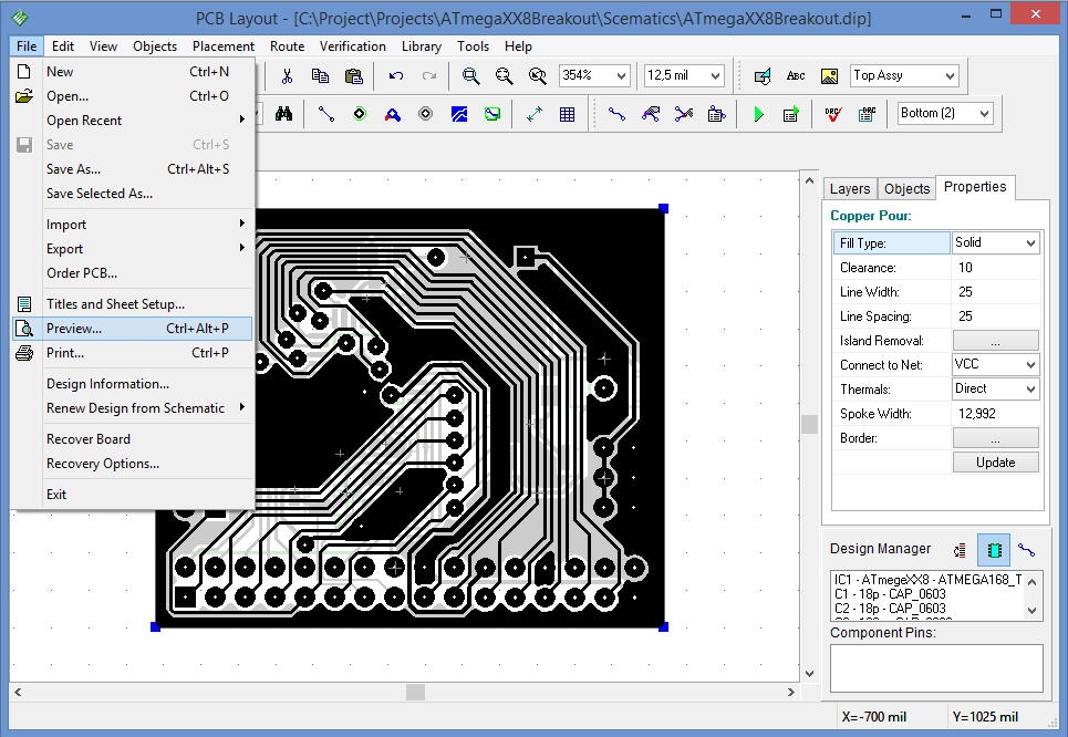 DipTrace support rasterizing and saving the layout to bitmap files. To do this open the Preview dialog.
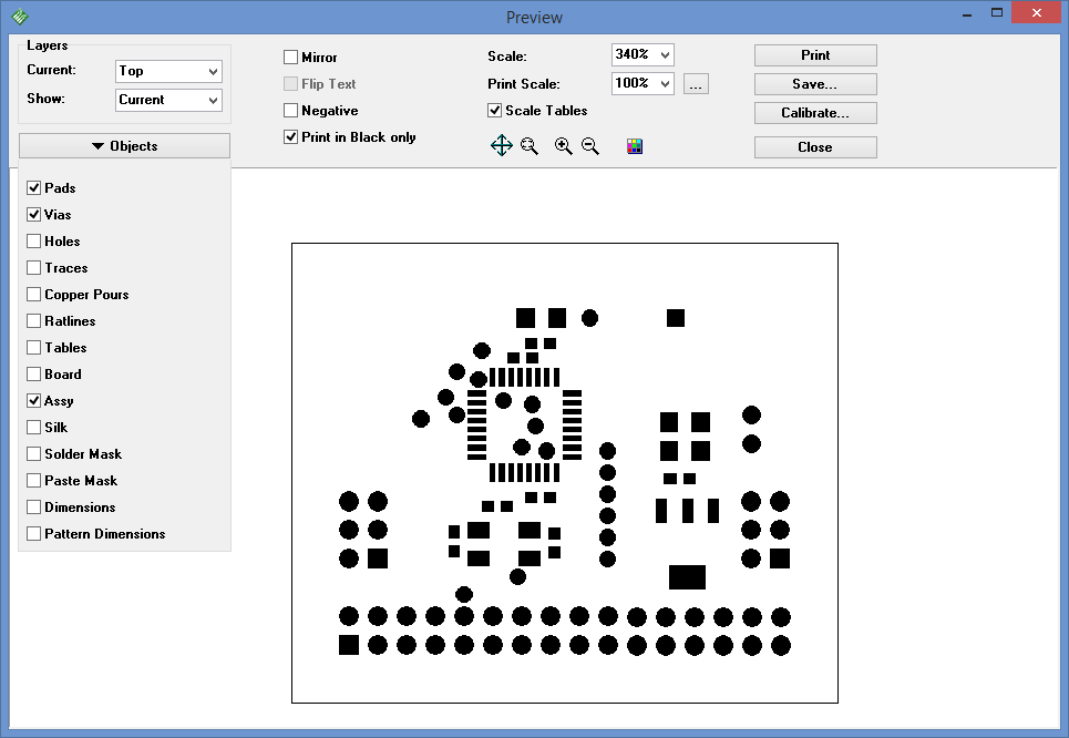
 Then expand the Objects menu and select the layers you want to include in the bitmap. Here we have selected all layers that should be part of the top signal mask (copper). Normally you would want to mirror any masks that is to be applied at the top of the board and invert any masks that is to be used with a negative photo reist. But I do that in the post processing of the files instead.To get rid of any repetitive work that had to be done in an image editor to prepare the masks, I wrote a couple of python scripts that do all the post processing for me using the python image library. The scripts handle mirroring, inverting, pad-swelling for the solder mask, removing silk-ink from pads/vias, convert DipTrace mounting-hole markers to etchable drill-marks in the copper, tinting to get optimal inkjet color for UV blocking, and tiling. More about this later.As you can see, I have included the “Assy” layer here. To make sure all the exported bitmaps have the same size and have the content placed the same I enclose the board with a rectangle in the top and bottom “Assy” layer. This is needed for the post processing scripts to work correctly.
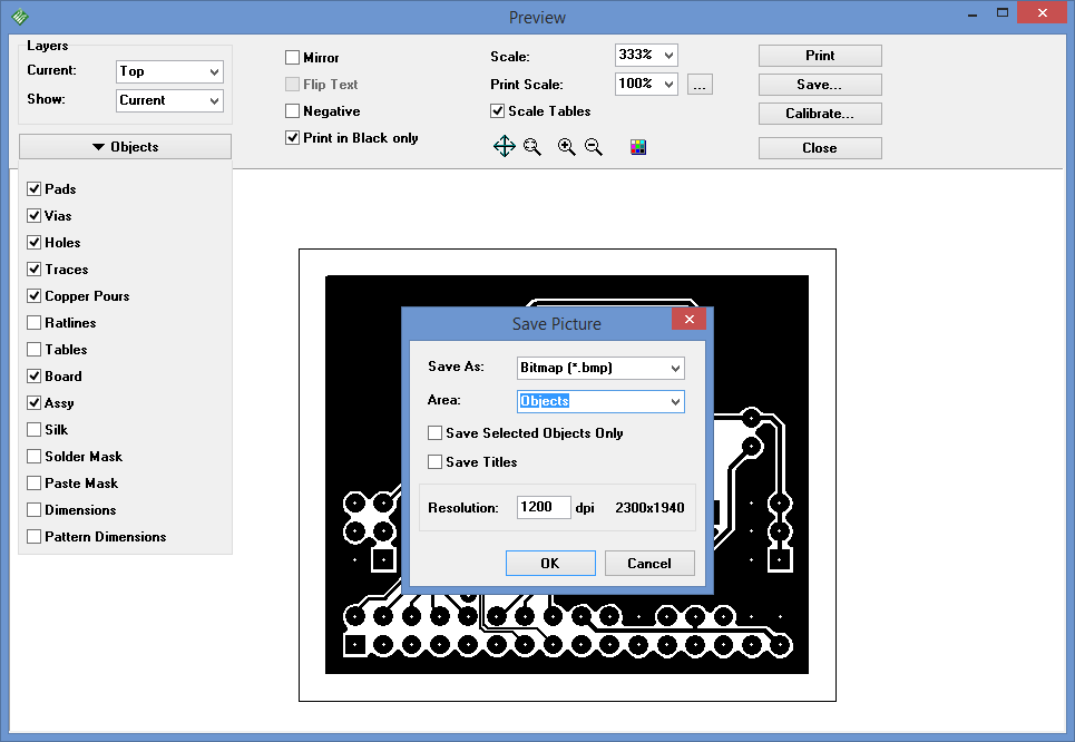 When the proper layers has been selected click the Save… button. This will bring up this dialog. Set Save as: to Bitmap and Area: to Objects. This will save a lossless bitmap just big enough to fit the content included. Then you should set resolution to match the DPI of the printer you are going to use. By having the “Assy” layer be the biggest and include it in all bitmaps they will all be the same size with all features positioned the same.
To save the bottom signal layer leave the layers alone and change Layers->Current to Bottom. Then save this into a second bitmap.
 Then we create the solder mask. Even though one of the layers are called “Solder Mask” that does not allow you to export a solder mask. I would have expected the pads + swelling to be included when saving this layer, but unfortunately that is not the case. The only things included by selecting this layer is objects hand-drawn into the “Solder Mask” layer. This is sometimes useful, and if you have done so, you should select the “Solder Mask” layer as well. I forgot to select it here, but I didn’t have any custom solder mask features in this board so no harm done.
To create a mask that exclude pads and vias I save a bitmap containing pads and vias but not holes. Then I post-process the bitmap to make swelling.
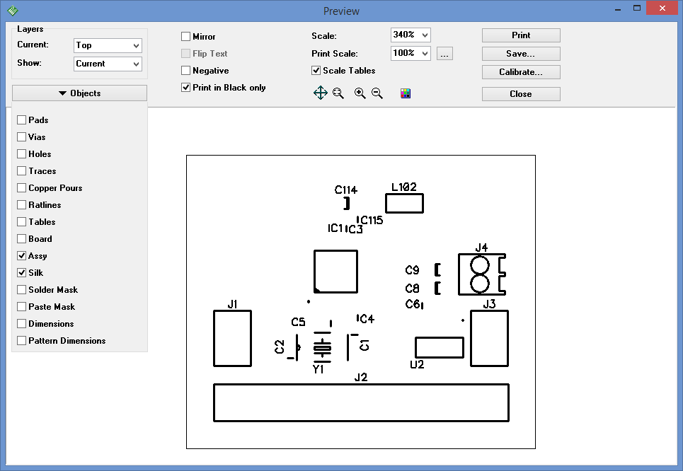 Create a silk mask the same way we did signal and solder-mask.
Post processing of UV masks (Custom python scripts)
When bitmaps are saved for top/bottom signal, mask, and silk I post process the bitmaps with the two python scripts I mentioned earlier.
The first script grabs the raw bitmaps for signal, solder-mask, and silk and do the following processing:
- Invert the signal and silk bitmaps to make them work with the negative photo resits.
- Add swelling to the solder mask.
- Stencil the swelled solder mask out of the silk layer to avoid having silk ink on pads.
- Locates any mounting holes and thickens some of their features so they survive etching and works as a drill-guide after the board has been etched.
This script has to be run twice for a double sided board.
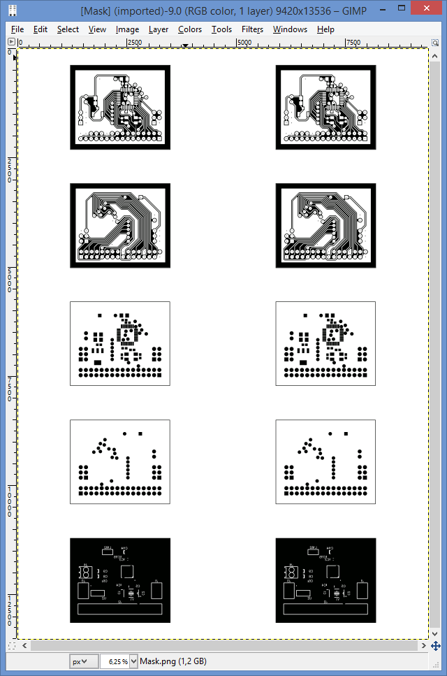
The second script handle tiling, mirroring, and tinting of the bitmaps. I use this to combine as much as possible on one or more A4 sized bitmaps. Each mask is included twice so they can be doubled up after printing for increased contrast.
The second script does the following:
- Place a number of bitmaps in a grid. The number of columns and rows to make can be specified. If more cells than bitmaps are specified multiple copies of each bitmap will be placed.
- Each bitmap can optionally be mirrored. This is used for all masks applied to the top of the board.
- Any black pixel in the masks are replaced with #000200. I.e. a hint of green. This force the inkjet printer to use yellow and cyan in addition to black which makes it block more UV that if printing with black alone. To find the optimal color I printed a gradient and did an exposure test. #000200 might only be optimal for my particular printer and my particular ink. Other brands might perform better with a different color.
Another nice script for creating UV masks from gerber files can be found [here]. It rasterize the gerbers and add the bitmaps to a PDF file. And it can do several useful modifications to the artwork. Like changing the drill sizes and other things that makes them more useful for a DIY PCB.
Printing the UV masks (GIMP)
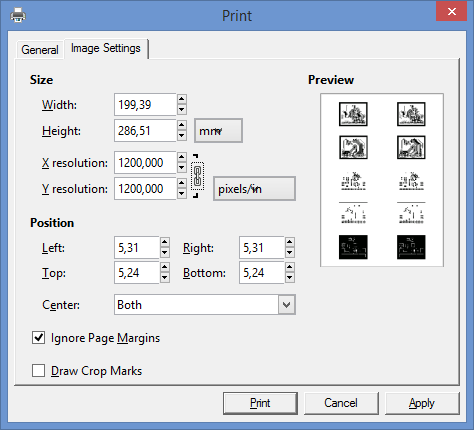
When the final mask bitmaps has been created I load them into GIMP and print them. I normally use Paint.net for any bitmap work, but the print feature in Paint.net is nothing but a sad joke. MS Paint work great for printing bitmap to size if the DPI in the image file is right. But I had issues making that happen with my python scripts so I installed GIMP to see if that would work any better. And it sure did. GIMP let you very easily specify the DPI to use. All you need to do to get the size right is to type in the same DPI when printing as you did when exporting the bitmaps.
Assembling the photo masks
 After all the bitmap processing is done I print the mask onto 80g/m2 tracing paper using an inkjet printer. I have also tried inkjet transparencies in the same inkjet printer, and laser transparencies in a laser printer. But tracing paper give the best result. The inkjet transparencies I have tried have too rough printable surface. This cause the high-points almost poke through the layer of ink and allow tiny dots of UV to get through in masked areas. The laser transparencies shrink in an unpredictable manner due to the fuser heat and makes it very hard to align two masks for increased contrast. With a perfect laser that didn’t make pin-holes and that applied enough toner to get by with one layer, I guess this would be the best solution. But I have no such printer in my possession.
Inkjet on tracing paper works great though. This also have issues with wrinkling and distortion when being covered by wet ink. But much of it return to normal when the ink dry. And what little remains does not cause any problems when doubling the mask to increase contrast. But I almost discarded tracing paper even without doing a proper test the first time I made a printout. Luckily I decided to give it a fair chance. When doubling the mask I first align one corner perfectly, and the opposite corner as close as the distortion will allow and glue that corner with a tiny drop of CA (superglue). Then I align the opposite corner perfectly and glue that as well. Then I do the same for the two corners in the other diagonal. After all this the mask usually will not lay flat on the table. It bends and curls due to the non-uniform distortion of the two layers. The amazing thing though, is that if you force it flat with a piece of glass (or with vacuum as I do when exposing) the flexibility in the paper makes the two masks align very nicely. Even for rather large masks. And the final total distortion is tiny enough to not cause any issues with aligning components with their patterns.
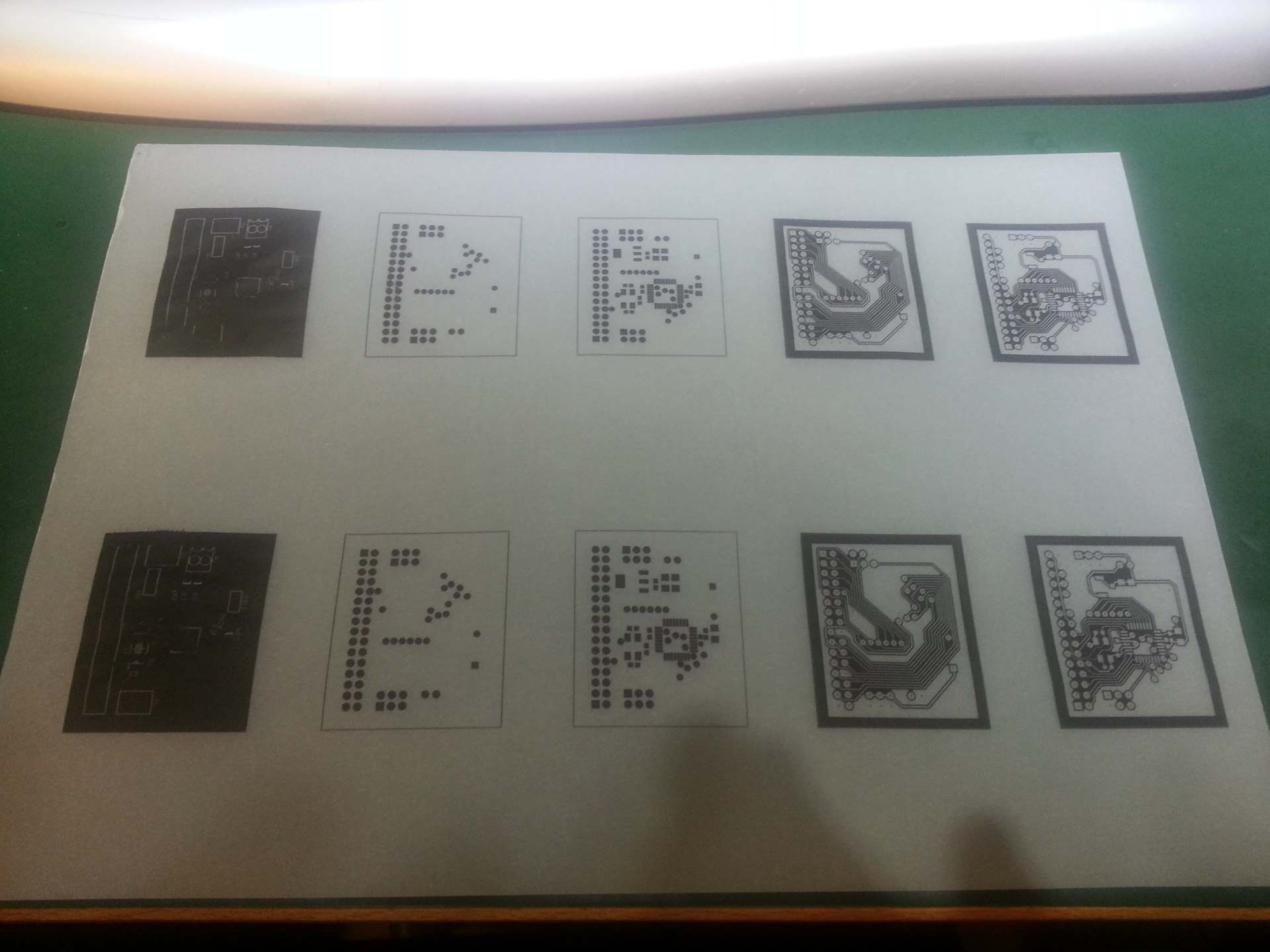
The printout pictured here have both signal, solder mask, and silk printed on it. Normally I only print the signal masks on tracing paper. For solder mask I use inkjet transparencies and I have not found a good way of applying the silk screen yet. So I normally don’t print a mask for the silk layer at all. But this time I was going to do some experiments so I printed them all.
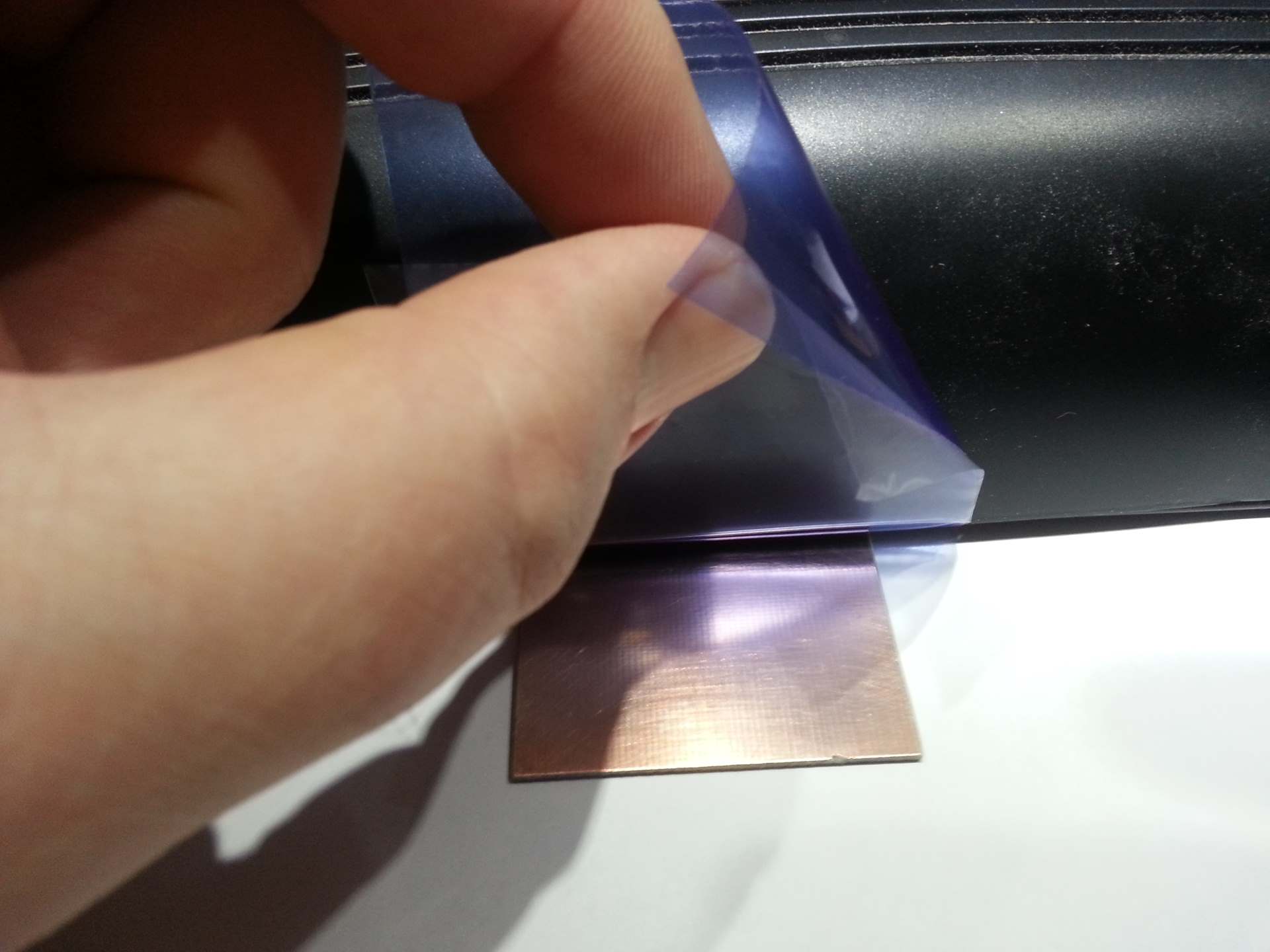
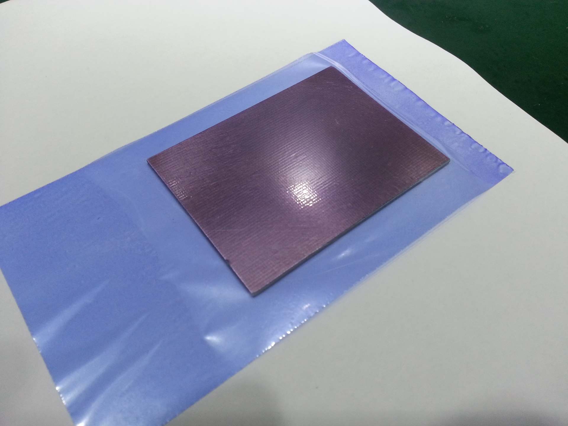
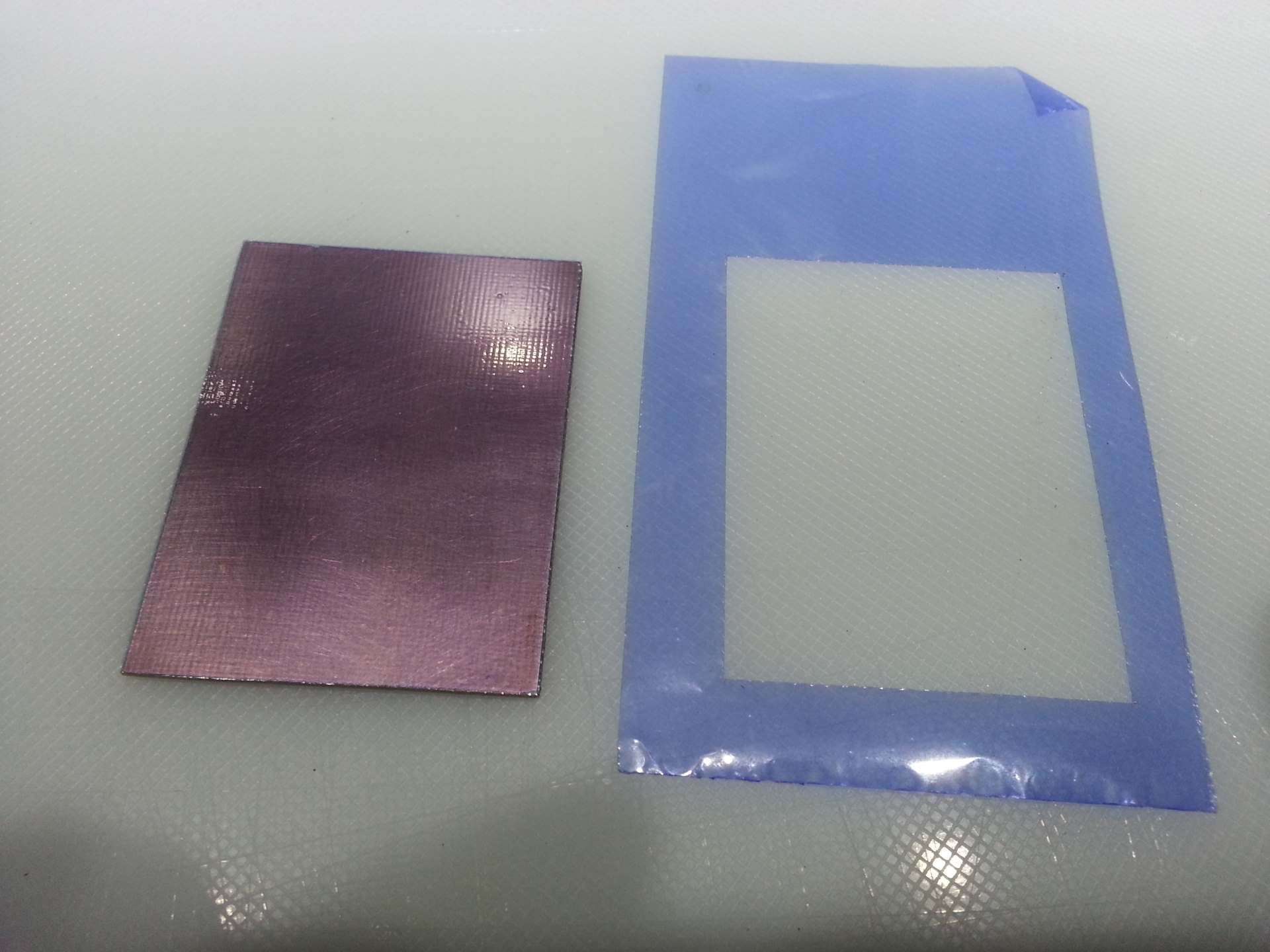
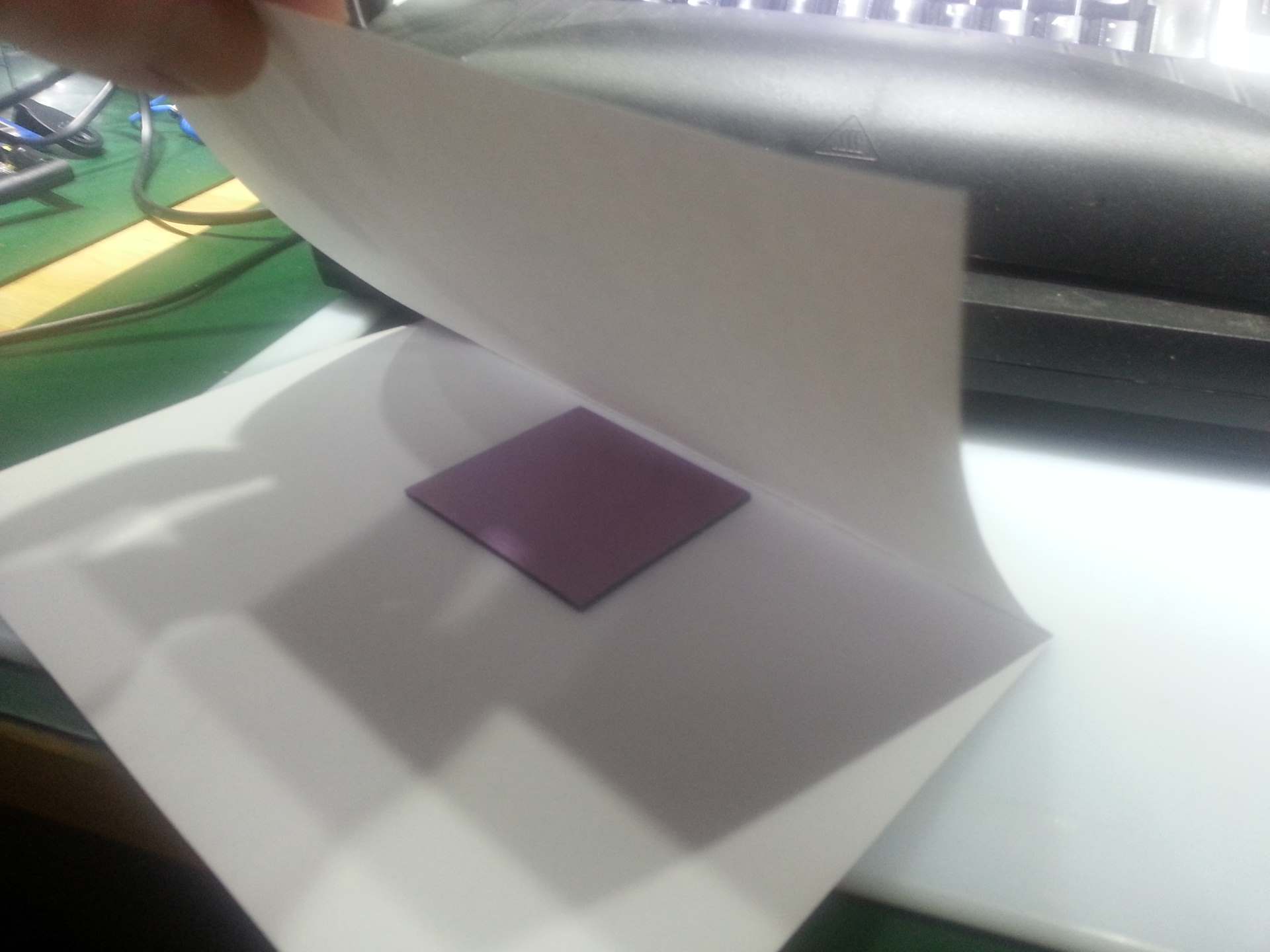
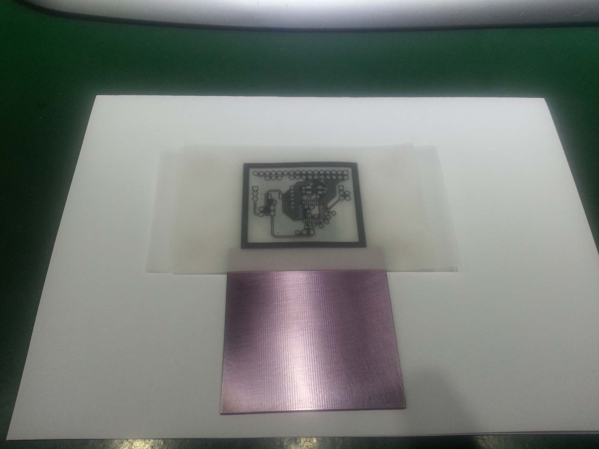 After making double masks for top and bottom layer I use the same technique to make a pouch that the sensitized copper clad can fit inside. The pouch is only glued in each of the four corners. This give close to perfect alignment between top and bottom layer.
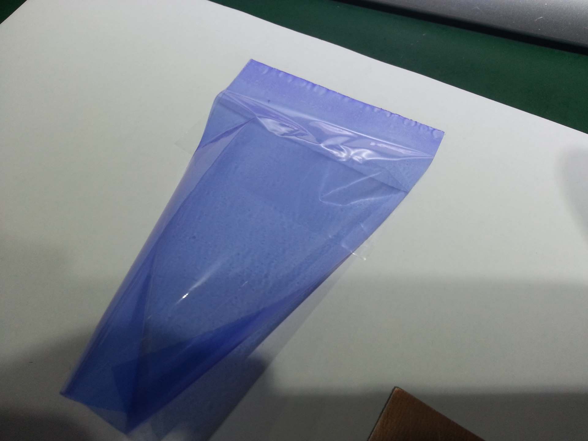
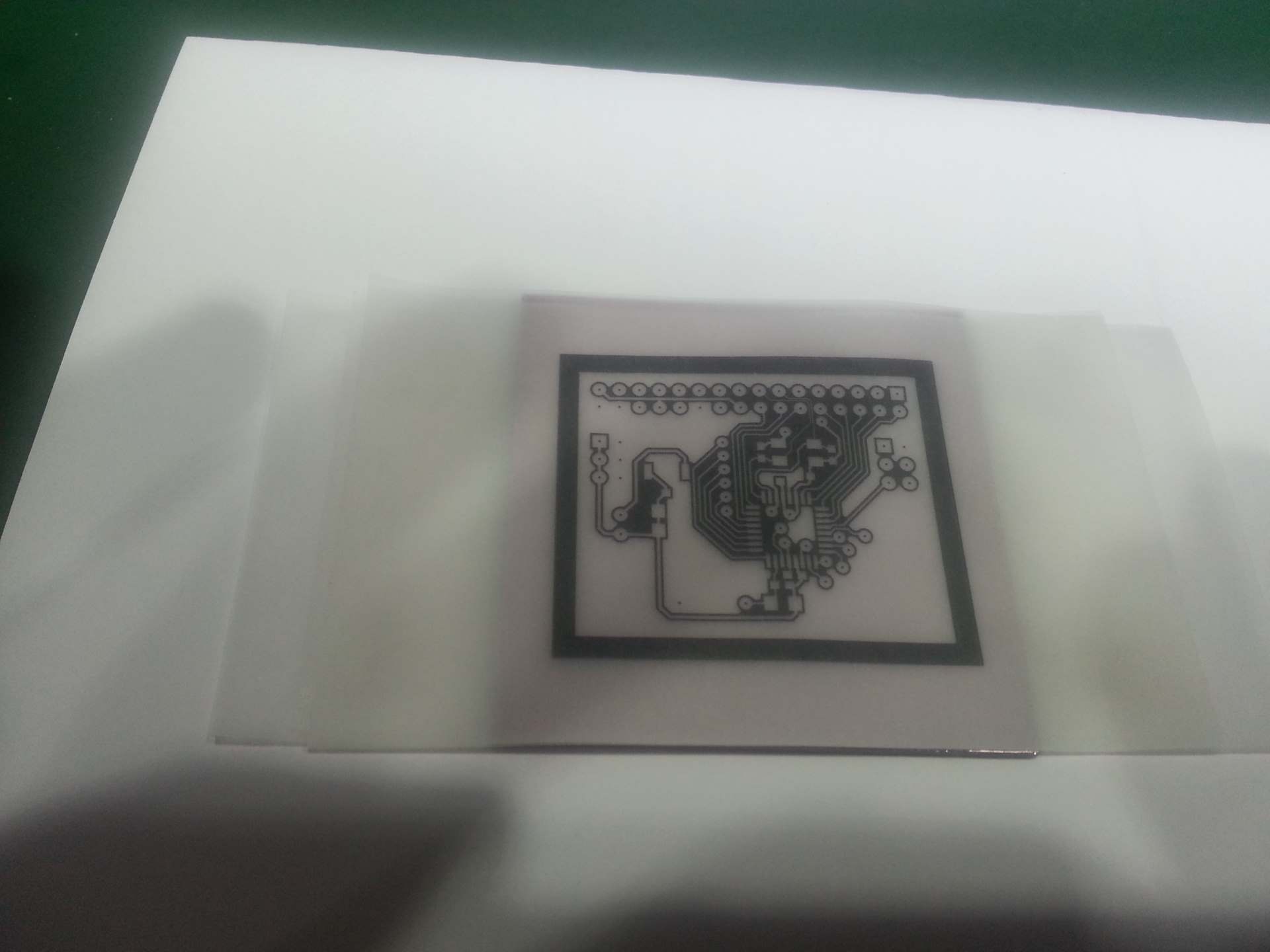 Here you se the pouch with a sensitized copper clad inside.
Applying dry film photo resist
This part took me quite some time to get right. Getting the dry-film onto the copper without wrinkles and without trapping air bubbles turned out to be tricky. None of the methods I found online seemed to work for me. I tried all kinds of techniques for getting the right tension as it went into the laminator to prevent wrinkles and air. I tried to apply it with fingers only before sending it through the laminator. I tried to apply it on a board sprayed with water. I tried to apply it with a board sprayed with a mix of water and alcohol. I tried to apply it submerged in water. About the only trick I had found described that I didn’t try was to go out and buy a professional vacuum laminator. None of the methods worked every time, or even often enough that it was acceptable. There was always wrinkles, or trapped air, or trapped water, or all of the above.
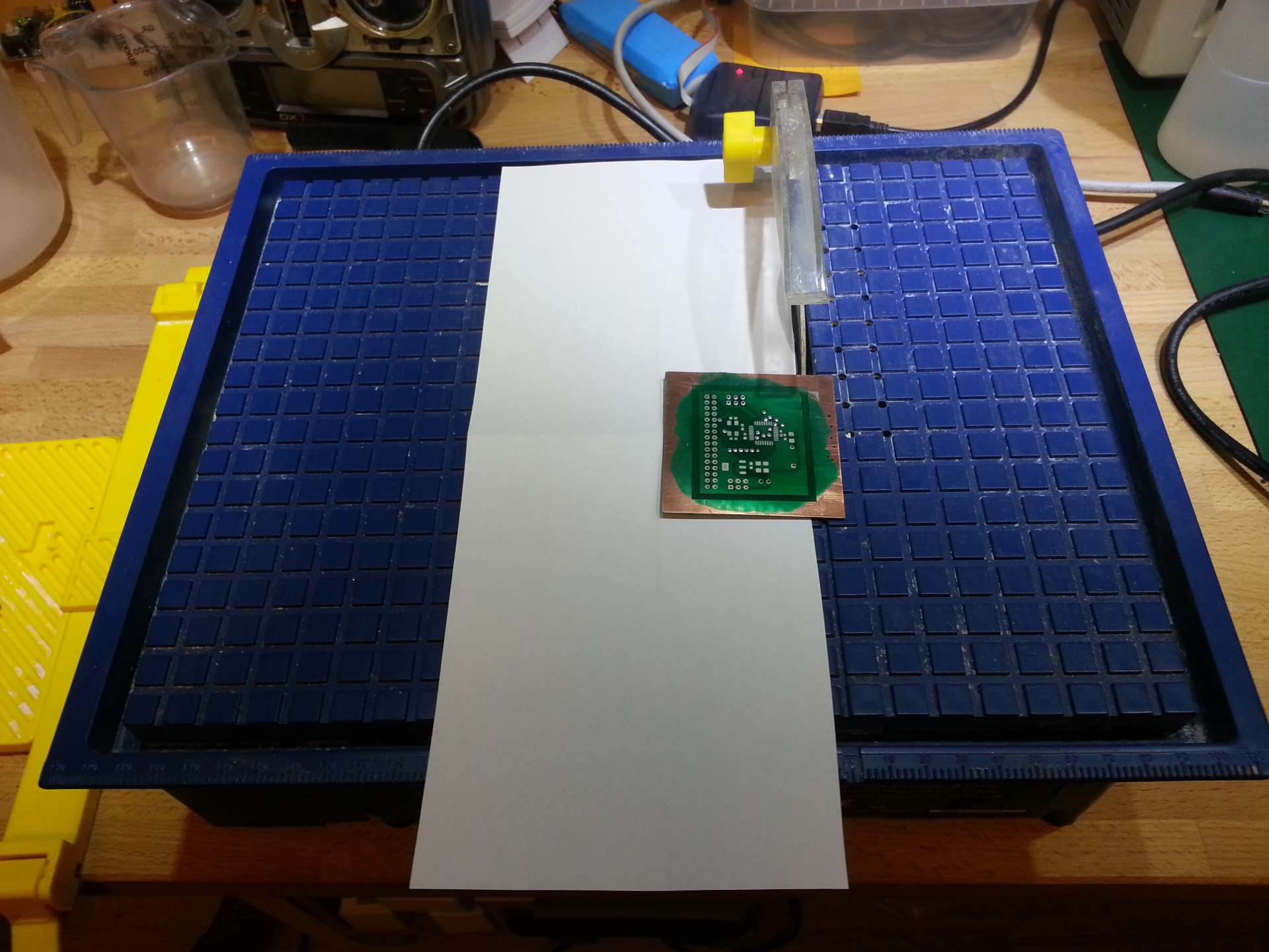
But eventually I found a method that seems to give 100% success every time. The board I make in the pictures below is not a very good example as it is tiny enough that just about any method would have worked fine. But I have also used this method to apply film to much larger boards (15x18cm double sided).
There is a few steps involved, but the whole process is pretty quick. And I have been getting very good results on first try after I started doing it this way.
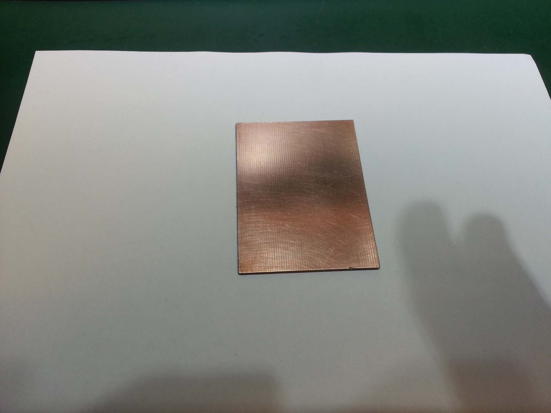
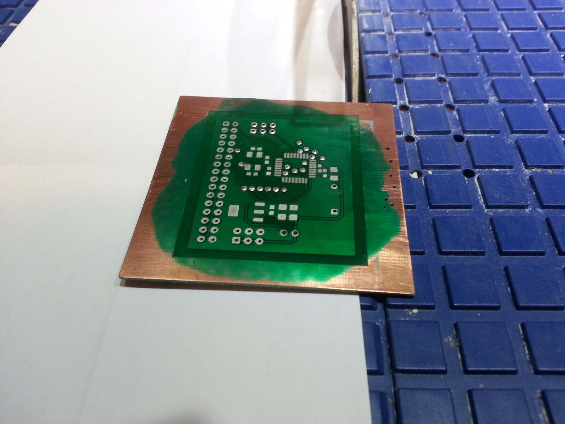
Copper clad after cutting and cleaning. I use soap-impregnated steel wool pads and alcohol to remove any oxides and other contamination from the copper before laminating. First I scrub it with steel wool under running water until it is shiny, then I wipe if off with alcohol. I have read that you should not use steel wool since it can leave behind iron particles that can cause issues. This has been random comments by people on the net that might or might know what they are talking about. I certainly don’t know for sure, but I have never had any issues, and it is by far the most efficient method I have tried. The most recommended method seems to be the green scotch pad sponges. But I find that it makes to deep scratches in the copper. So I will stick to the steel wool for now.
When the copper clad is reasonably clean it is time to apply the resist film. I start by pealing back one of the protective layers a little. One piece of scotch tape on each side makes it easy to start the peal. After pealing the plastic back a couple of centimeters I tack the exposed end to a piece of paper.

Then I prepare the laminator. I put something in front of it to support the paper as it goes in. A plastic box in this case. I have two laminators that I use for this process. Both are standard cheap poach hot roll laminators, but one of them is modified a bit for this purpose. First of all, it is not so hot any more. I have cut the wire to the heater to disable it. And I have also replaced the geared motor inside with one that run at 1/6th the speed. Both the laminators use the same kind of motor even though they are bought in two different countries many years apart. And it seems that they also share the motor with a lot of micro wave ovens. And those can be found quite cheap on eBay. Only problem is that the micro wave motors does not have a defined rotational direction. They start in a random direction each time (1-phase syncronous motor). So now I often have to start the laminator multiple times before it run in the direction I want. Annoying, but not a show stopper.
It is the modified cold and slow laminator I use for the initial application of the film. One major problem when applying the film is that air bubbles tend to get trapped between the film and the copper. The low speed and lack of heat pretty much eliminate this problem, as the film don’t stick very well to the copper and the slow speed give the air time to escape.
Then I stick the paper with the film tacked to it into the laminator. Under the film I place the copper clad. Between the film and the copper clad I place a 2mm thick carbon fiber rod.
The carbon fiber rod follow the the board into the laminator until the edges hit the sides of the laminator. It will then give a bit of tension to the film and make sure it don’t touch the board until hit by the roller. This further ensure that no air is trapped under the film. The protective film is folded the other way so it can be grabbed as the stack goes into the laminator.
As the stack goes into the laminator I hold back the protective film. This gives a bit of tension to the film and keeps it from wrinkling. It should separate as close to the entry of the laminator as possible to reduce the danger of dust getting trapped between the film and the copper clad. If you try to remove the entire protective film upfront a fair amount of static electricity is generated and unless you are in a clean-room you are pretty much guaranteed that the result will be ruined by dust.

The stack exiting the laminator.
This is how it looks after it has been through the laminator. The film stick fairly well to the copper clad at this point, but can easily be pulled away from the paper.
After pealing it off the paper I trim away the excess film. Now it is time to flip it over and repeat the process for the other side. If it is a double sided board that is.
When both sides have been covered using the cold/slow laminator I wrap it in paper and send it a couple of times through an unmodified hot laminator to make the film stick properly to the board. Wrapping it in paper is a good idea to avoid smearing up the laminator rollers with sticky photo resist.
Exposing & Developing
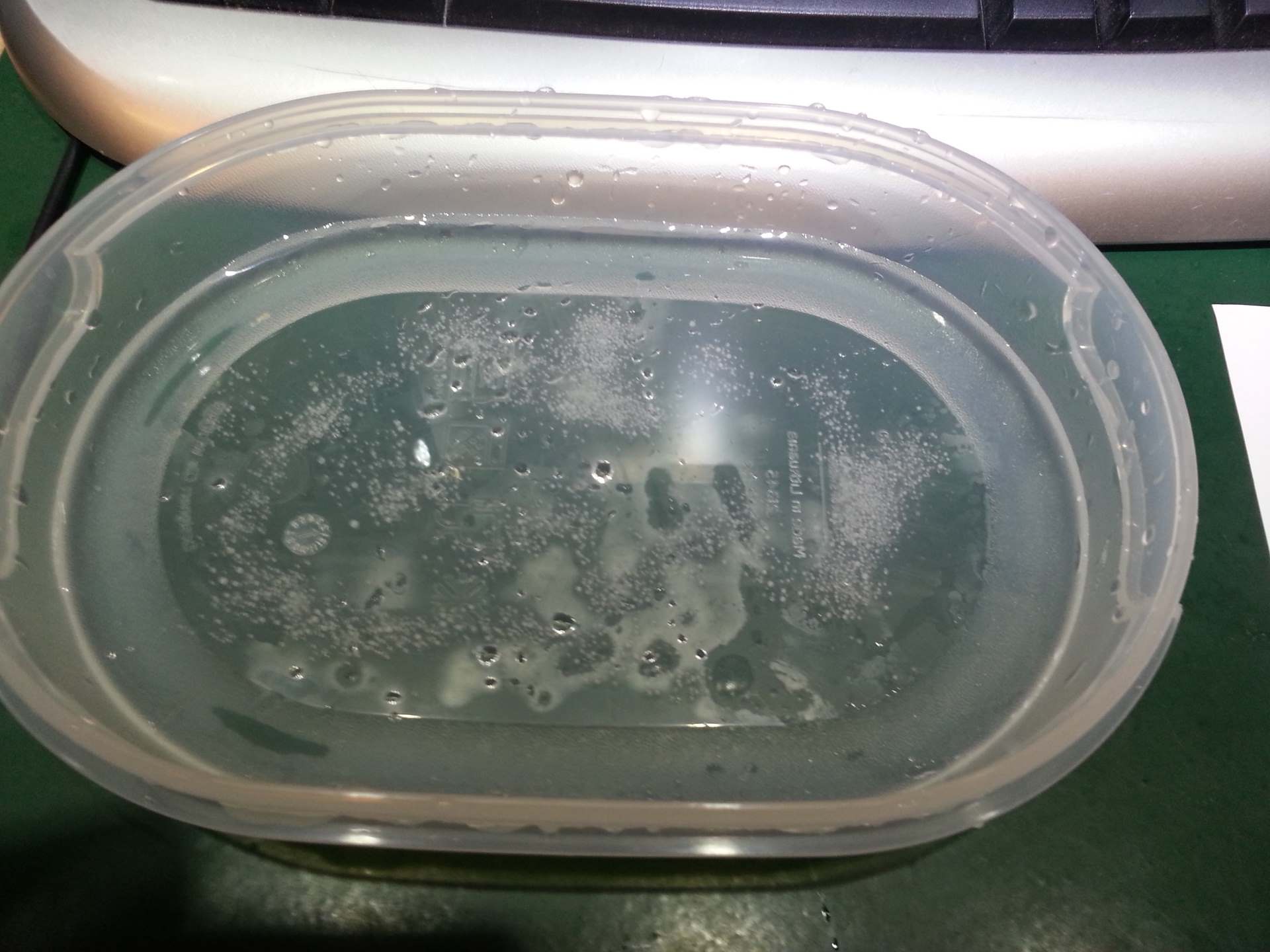
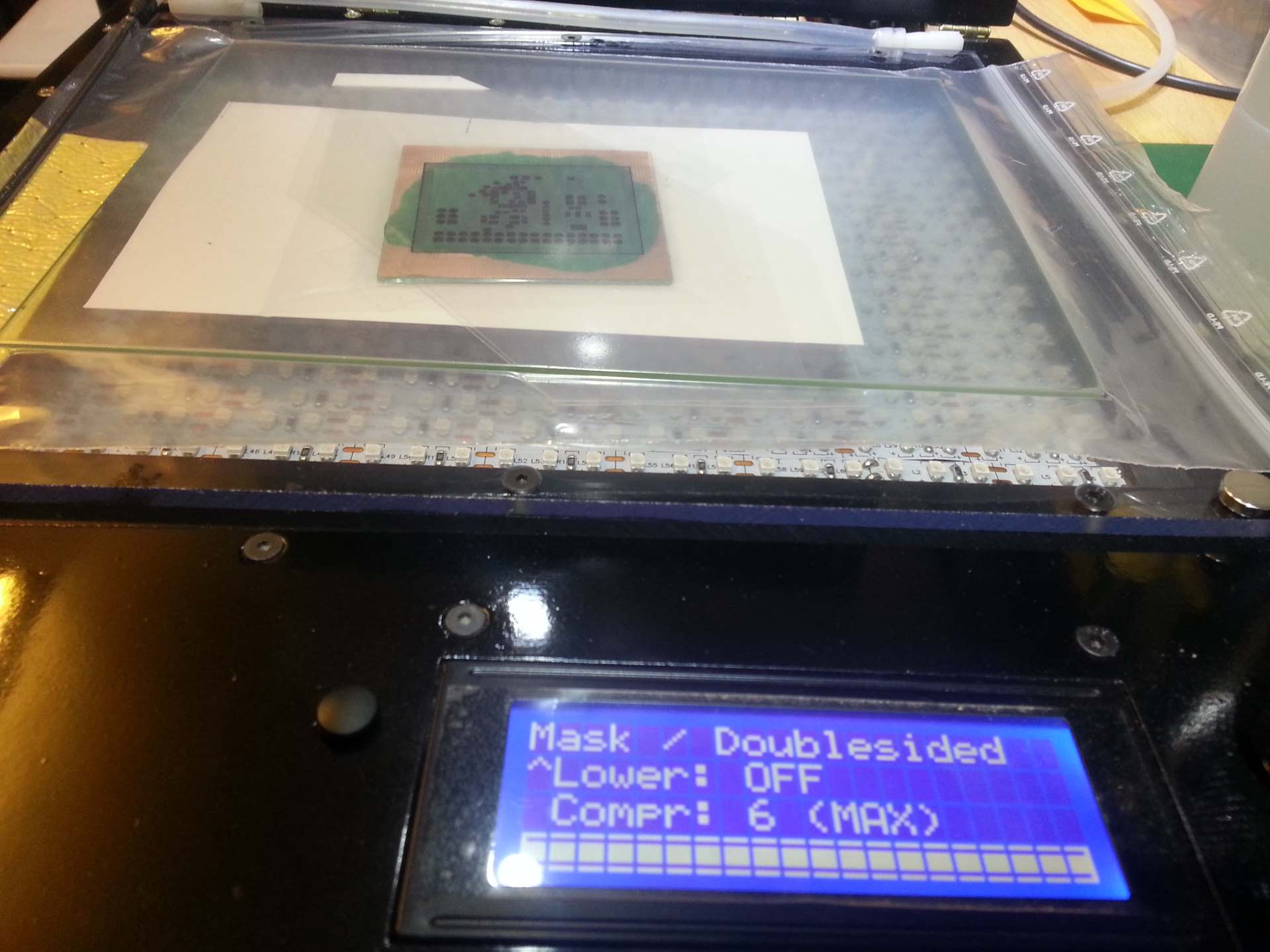
To expose the sensitized copper clad I use my home built double sided UV exposure unit with a built-in vacuum pump. The same can be done with any appropriate UV source and most any vacuum pump. Before I built this I used a UV nail-curing lamp and the vacuum pump from a manual pick-and place pen (which looks and sounds just like most aquarium pumps, but it sucks instead of blowing).
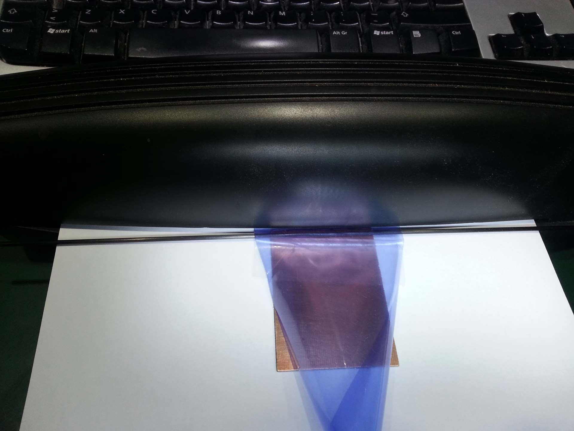
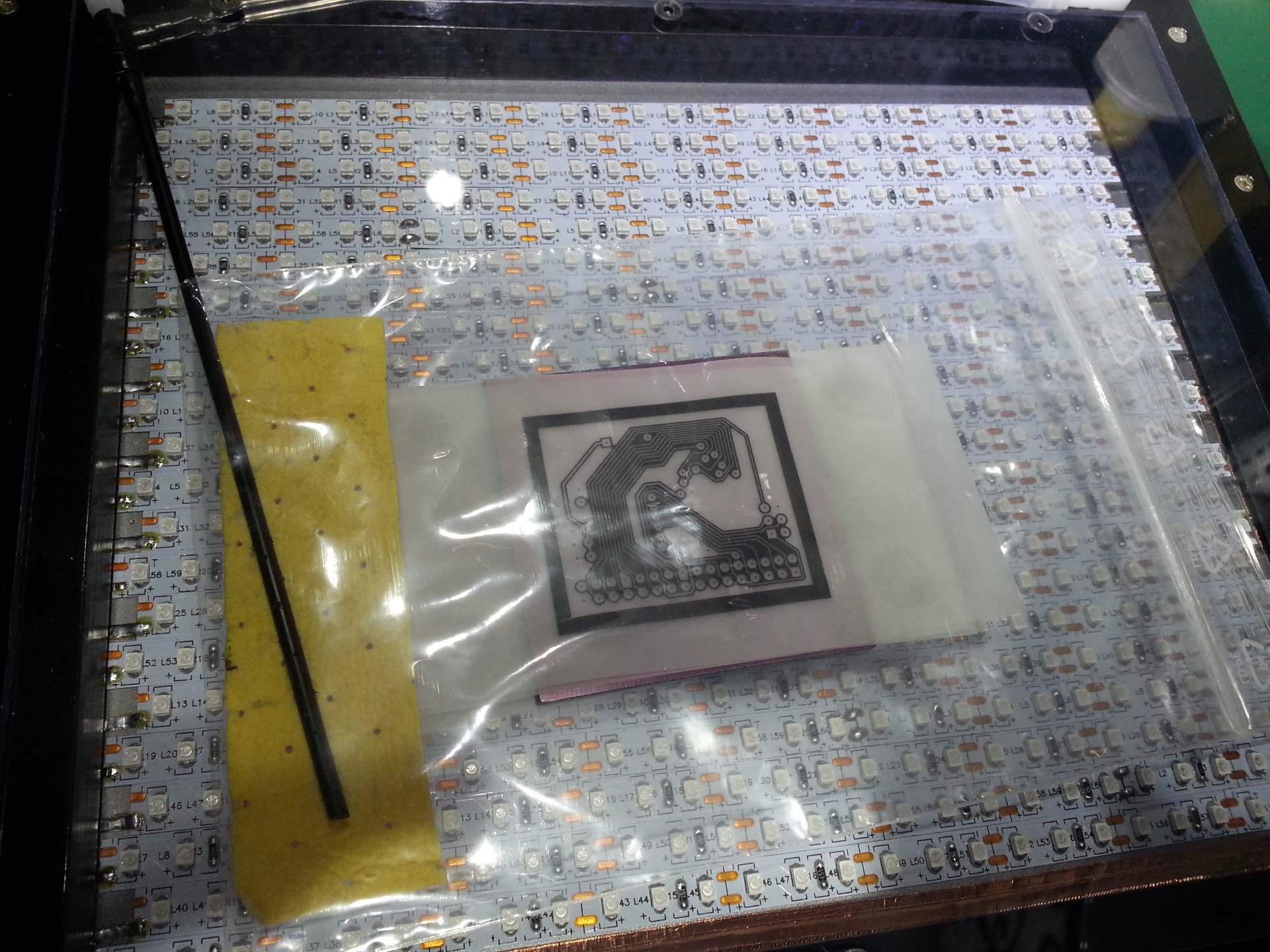
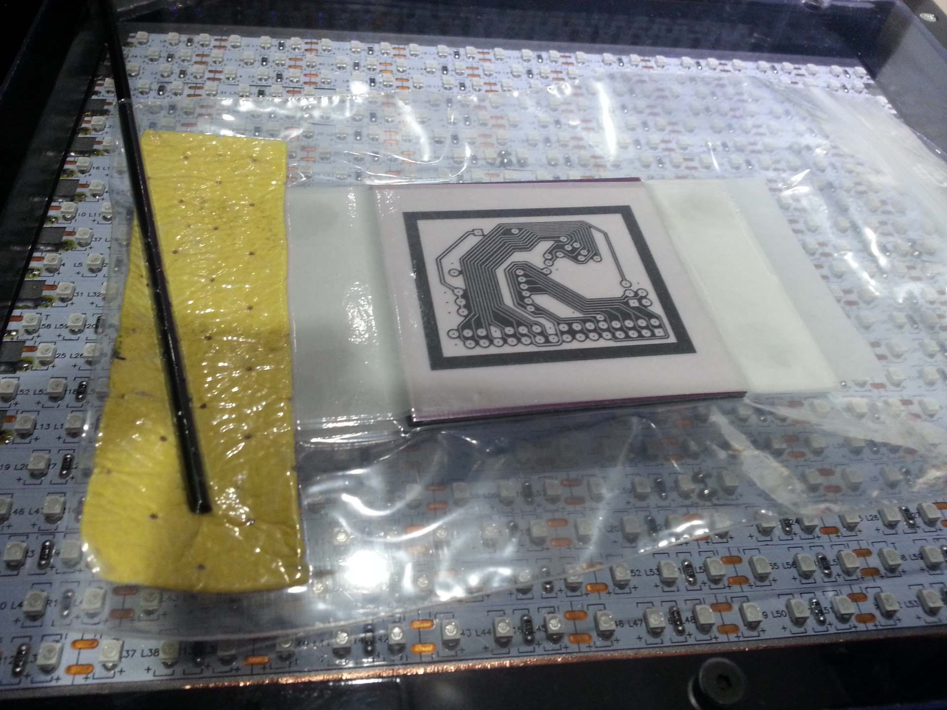
The UV exposure box is much more convenient though. To make sure the photo masks are firmly pressed against the copper clad while exposing I put it inside a zip-lock bag and evacuate as much air as my vacuum pump allows. To be able to evacuate the air I cut a tiny corner of the bag and insert a thin plastic tube through it. The plastic tube is perforated in one end, and have a hose fitting in the other. Inside the bag I make sure the perforated end of the tube rest on a piece of fabric and that the UV mask overlap the fabric. This ensures that the plastic is not completely sealing anything up before enough air has been evacuated. The cut corner seals it self well enough due to the vacuum alone.
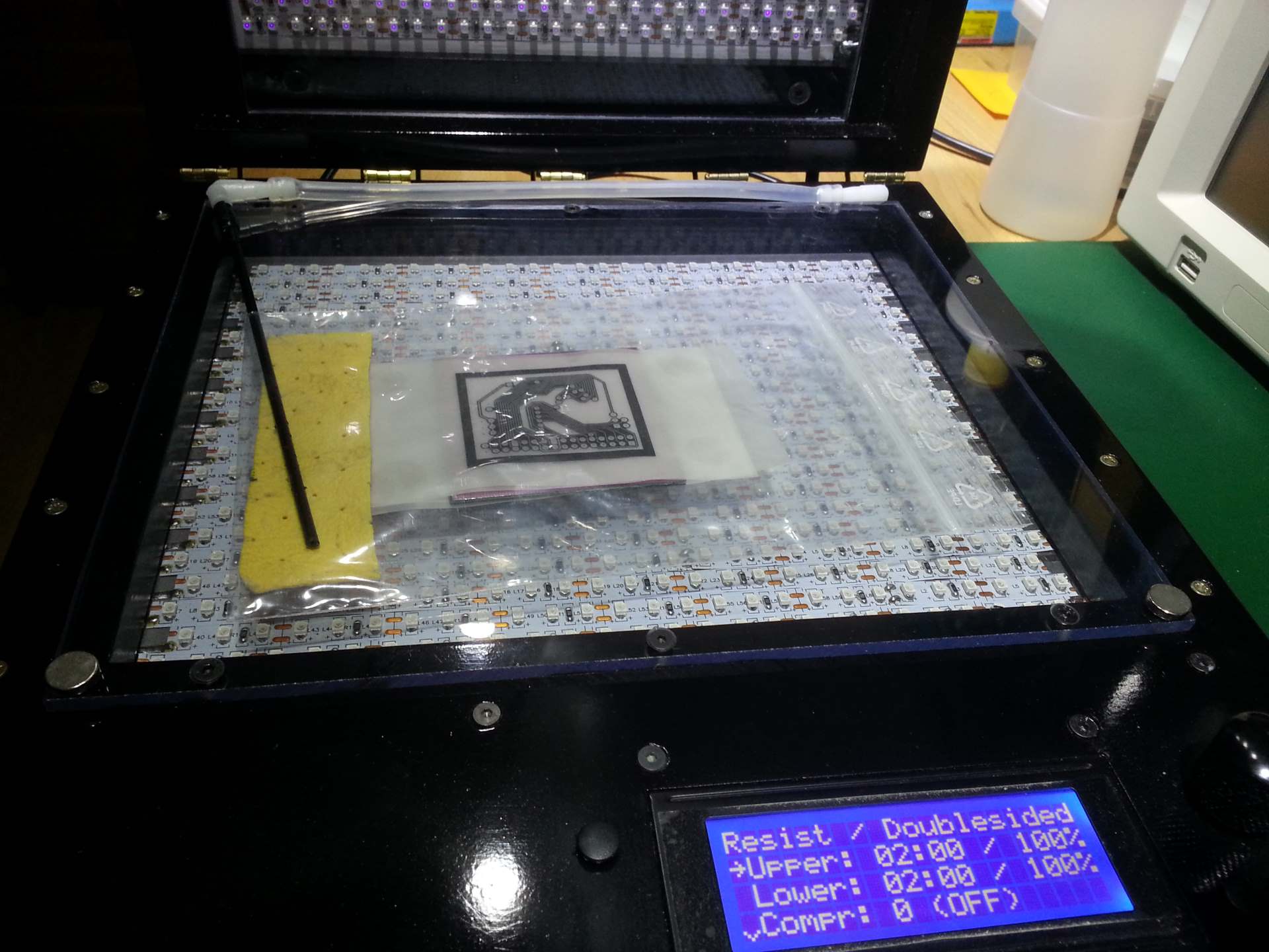 This is how it looks with the vacuum bag placed inside the exposure unit and connected to the internal vacuum nipple.
 After placing the bag and hooking it up I start the vacuum pump at the slowest speed where it will run without stalling. This give me enough time to stretch out any wrinkles in the plastic before it is pulled in to hard and forms permanent creases.
 When the plastic rest smoothly against the UV mask I turn the vacuum up to 100% for a while to evacuate as much air as possible, and then slow it down to 70% to reduce noise and pump-strain while still maintaining an acceptable vacuum.
Then I close up the lid and start the radiation. Radiation time for this setup is 2 minutes. This will vary depending on the photo resist used, the opacity of the tracing paper, and of course the power of the UV source.
To calibrate the exposure time I exposed a similar board to what you see here but starting with most of it covered with aluminium foil. Then every 15 seconds I pulled the foil back about 5mm until the hole board had been exposed. Then I developed it and calculated the total exposure time of the area of the board that had received the most UV but still allowed masked areas to easily dissolve in the developer.
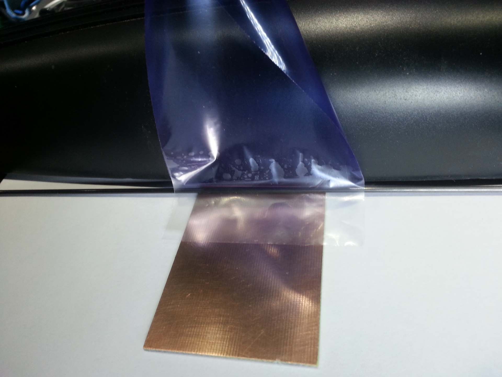
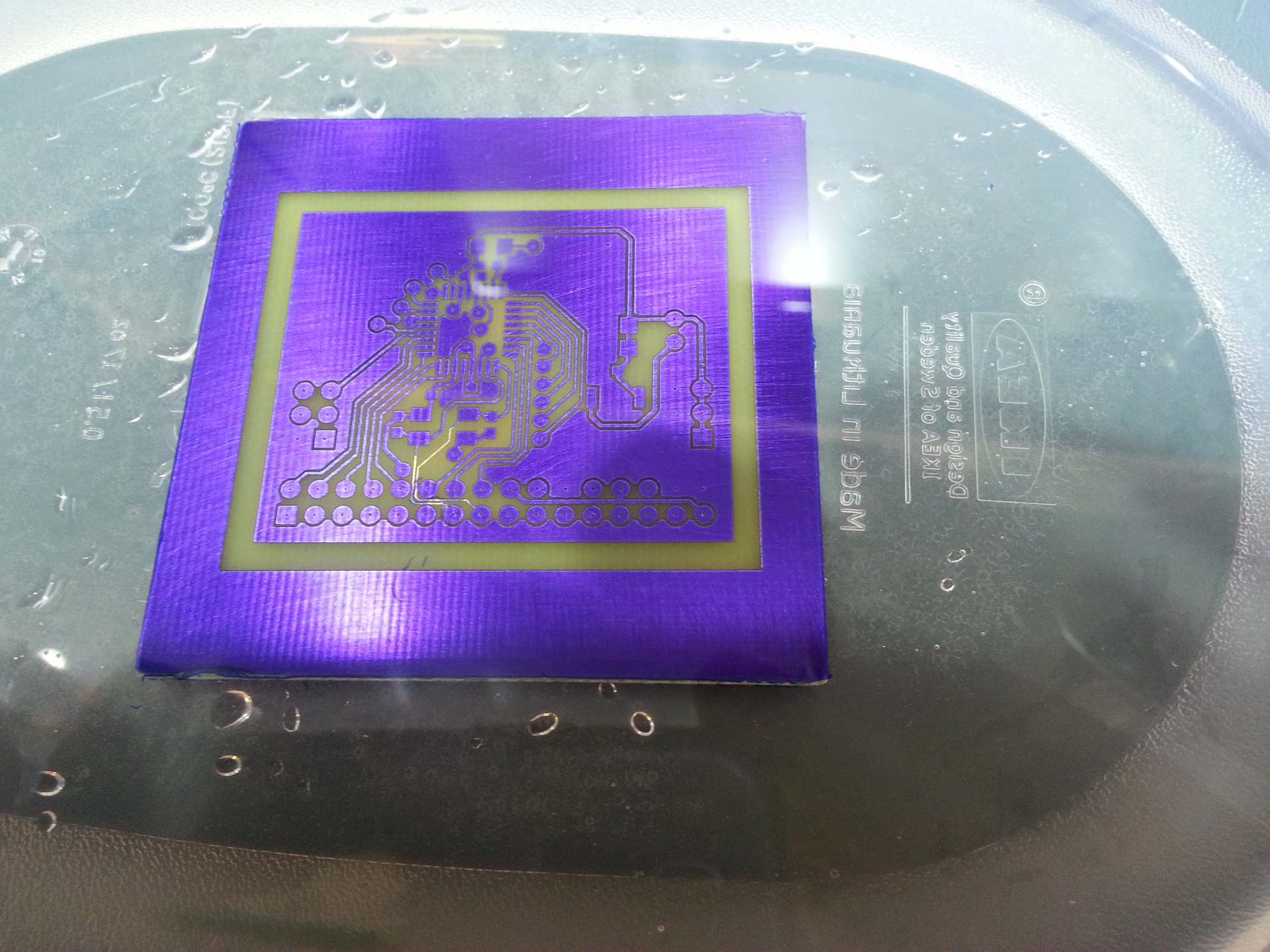
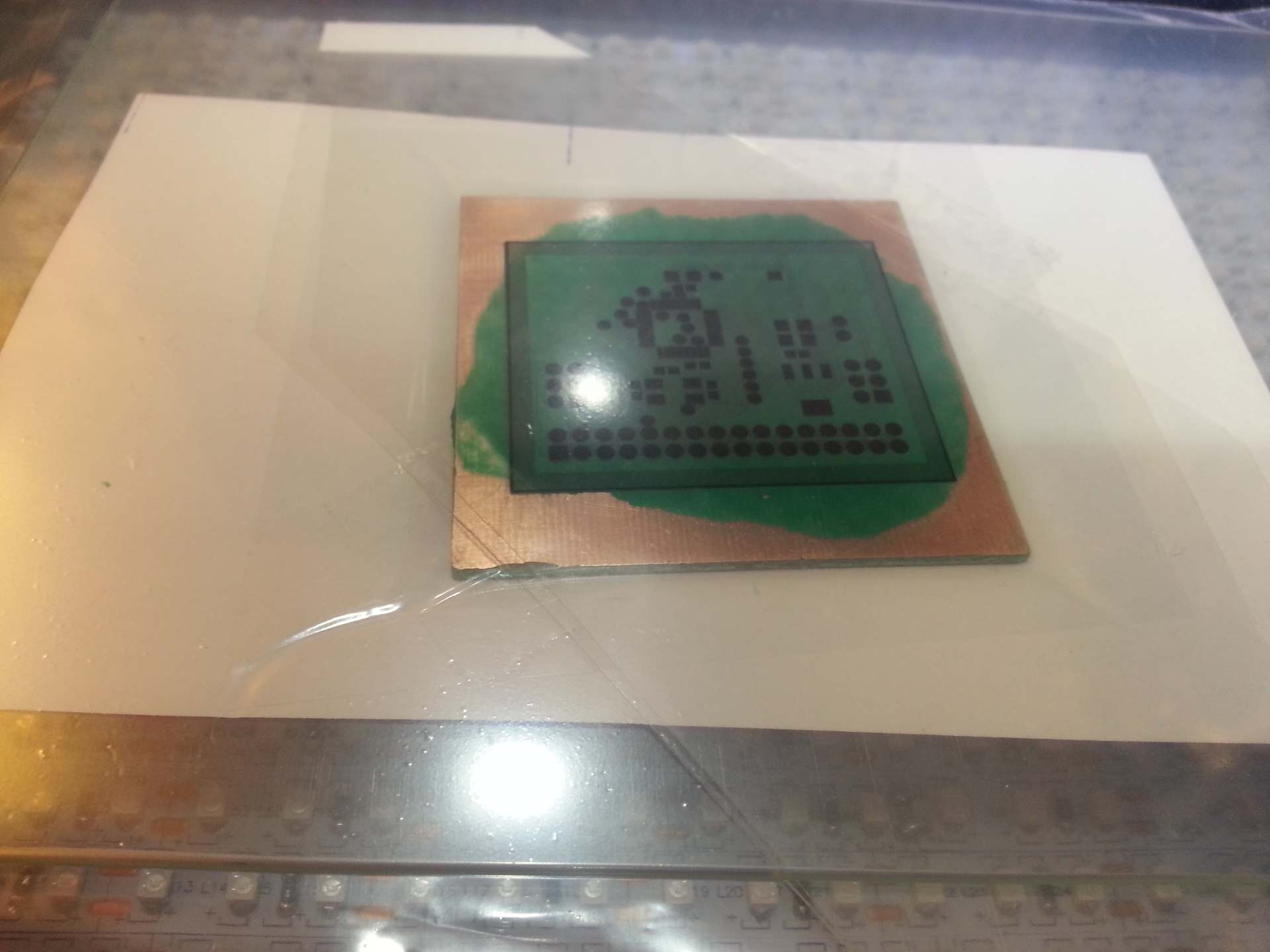
 This is how it looks fresh out of the UV exposure unit. At this point the protective plastic is still attached to the photo resist. This film should not be removed before exposing as oxygen will inhibit the polymerization of the resist and can cause the hardening to fail. This does not seem to be a problem with shorter wave lengths but can be an issue with the 395nm light produced by my LED based exposure unit.
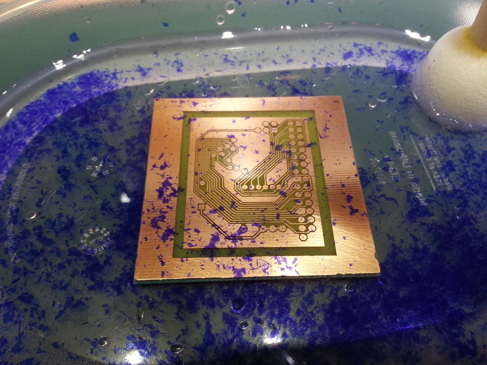
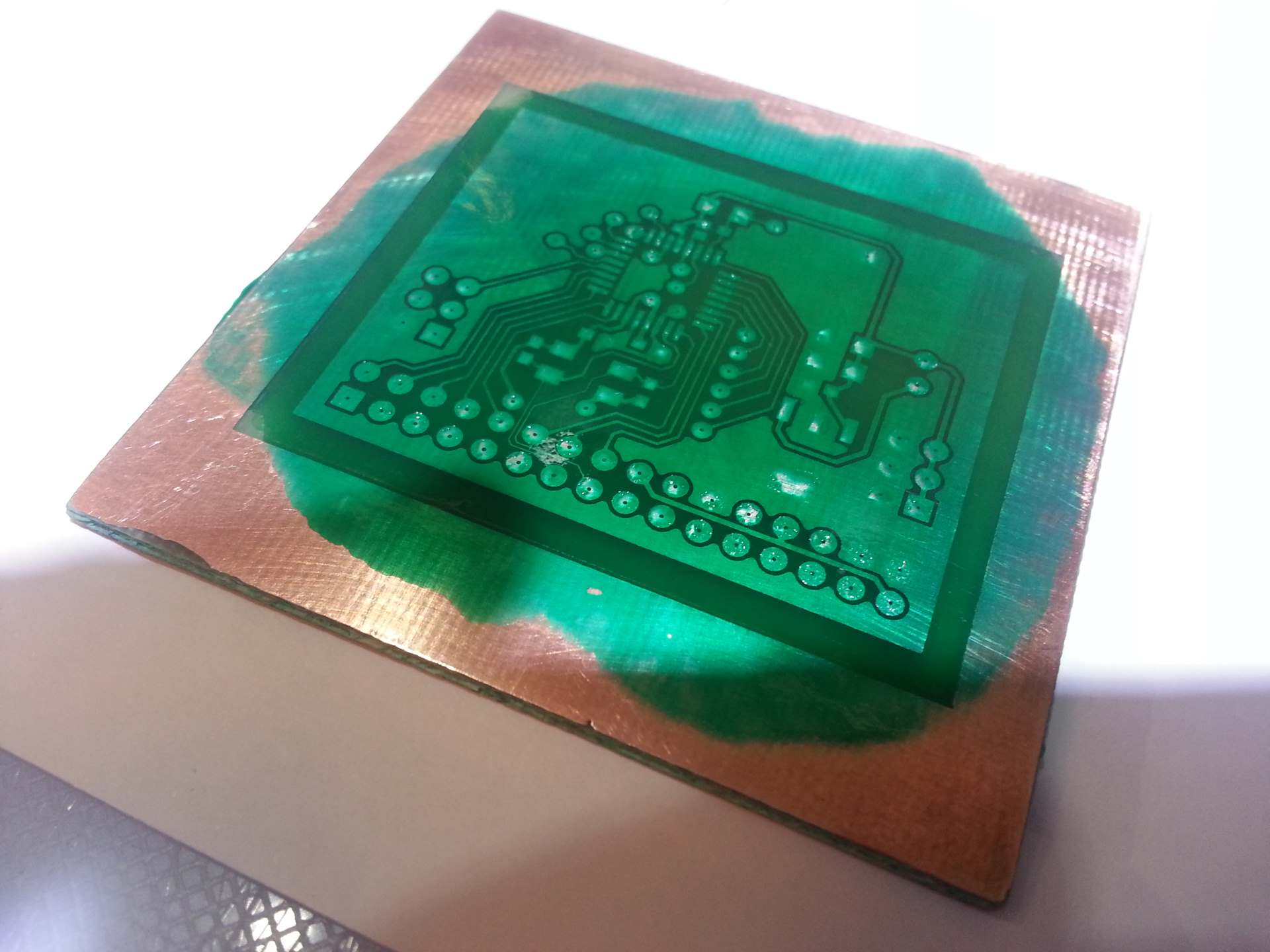
 And this is how it looks after being developed.
To develop the board I use a mixture of 0.85% Sodium Carbonate (Na²CO³) dissolved in deionized water. I simply drop the board in a plastic container filled with enough developer to easily submerge the board. Then I gently swipe the board with a sponge brush until all unexposed resists has been removed.
When I think it is done I take it out and let it dry. If some areas is under developed it will show up much easier when dry as the half dissolved resist will turn milky white. If this happen I swipe the areas a bit more with the developer soaked sponge brush. When all unwanted resist is gone I rinse it in running tap water while scrubbing it quite firmly with my fingers to make sure it is properly cleaned.
After it is fully dried I pan over it a few times on each side with my digital microscope spotting for breakage in the resist or under developed areas.
Etching
To etch the board I use my home built vertical etch tank filled with sodium persulfate (200g/L). The tank has a built-in heater and is bubble agitated.
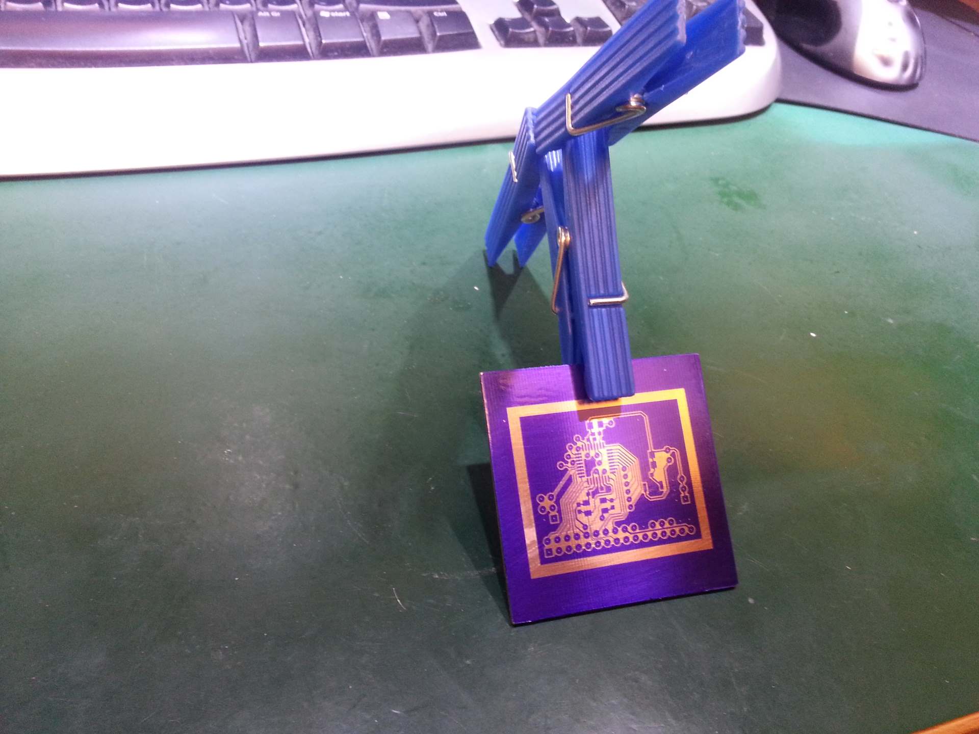
Normally I drill two tiny holes in the PCB and suspend it in fish lines. But this time I decided to try something else. Cloth clamps! Yes, I know. Metal spring and etchant… Hope I can find an all plastic clamp one of these days. But I decided to give it a go anyway. Maybe I would luck out and the spring was made from an alloy totally resistant to sodium persulfate? Either way I gambled that it would at least last long enough to finish this one board. And it did. It changed from nice and shiny to rather dull, but didn’t seem to loose much mass. More worrying though was that my fresh batch of etchant turned into a slightly murky green rather than the normal translucent blue after the first use. Might have to rethink the whole cloth clamp idea. It was much more convenient than the fish line though.
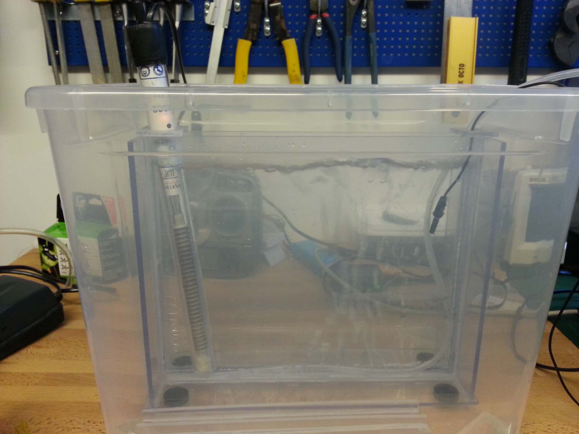
This is the etch tank with the heater on and the bubble compressor running at low speed to make the etchant circulate. Originally I used an aquarium pump to provide bubbles, but now I connect it to the outlet of the vacuum pump built into my UV exposure unit. This gives much better control over the air flow and also have a much higher maximum flow. I might have to build one into the etch tank one day. The MCU used to control the compressor could also be useful for controlling the heat a bit more precisely than the thermostat built into the heater. To many projects to little time.
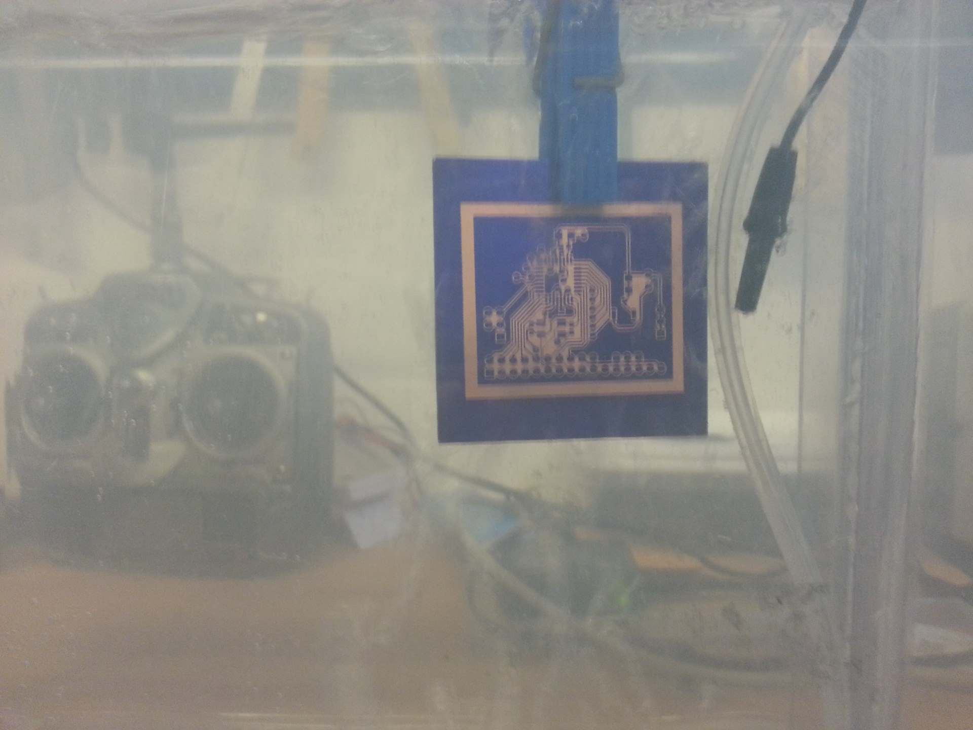
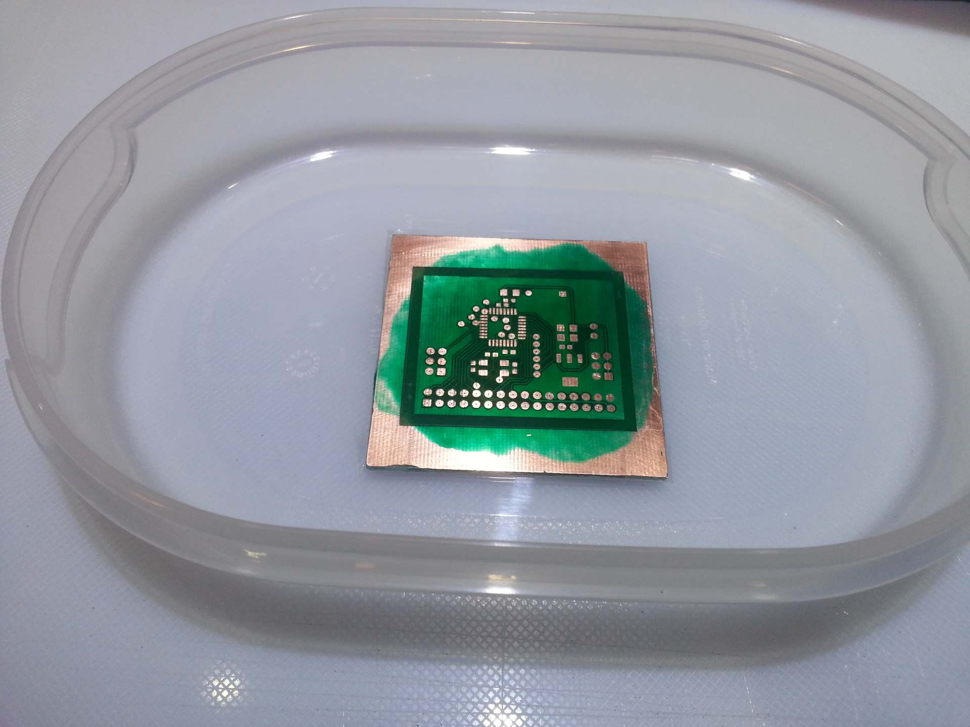
Here you see the PCB submerged into the heated and agitated etchant.
After a couple of minutes the unwanted copper has been eaten away and the board looks like this. The inside of the 0.3mm drill guide holes are usually the last to let go. So they are a good gauge for when the board has been fully etched.
Stripping
Now we need to strip the resist off the copper. To do this I mix 1.5% Sodium Hydroxide (NaOH) with deionized water. Normal tap water should work fine too. Be very careful when dealing with this stuff. NaOH quite readily dissolve flesh and eyes. Use appropriate protective gear!
Then I drizzle the NaOH crystals into the water and wait for it to fully dissolve. The water is at room temperature.
Shortly after being submerged the thin traces start to loose the resist.
A bit later all the resist has cracked up and are floating away from the PCB. I use the same sponge brush to help this process as I use when developing.
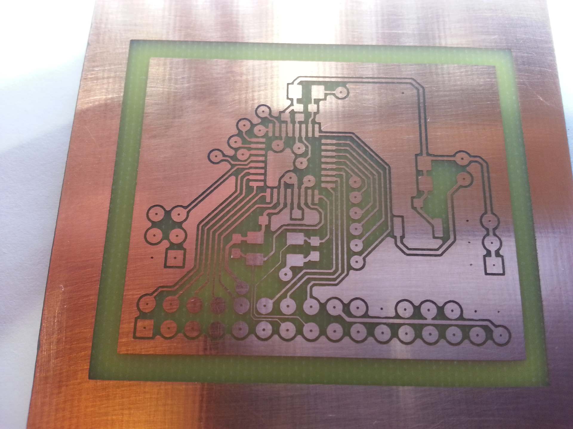
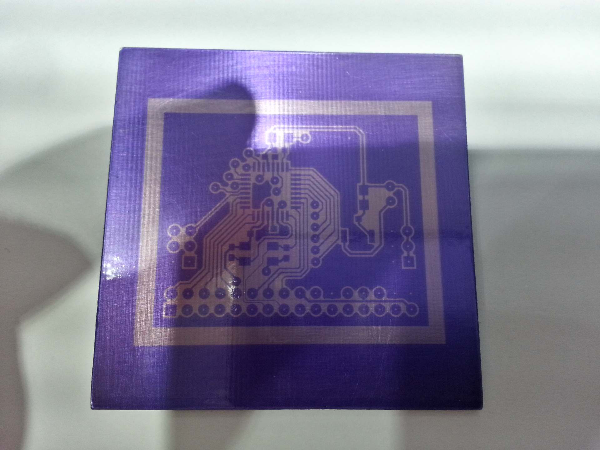
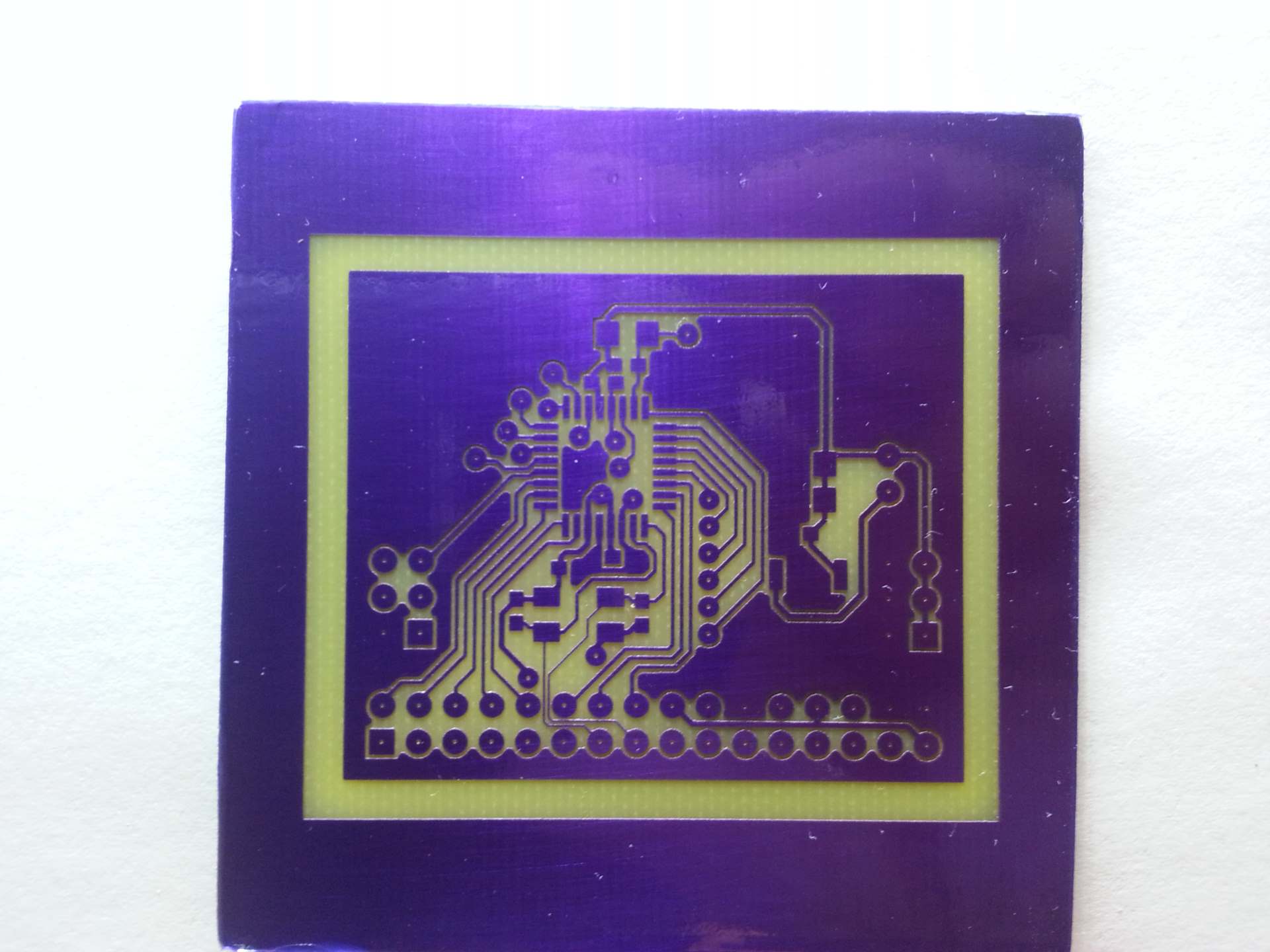
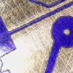
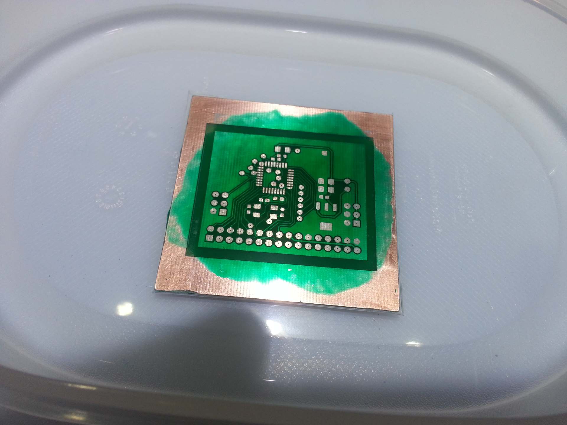
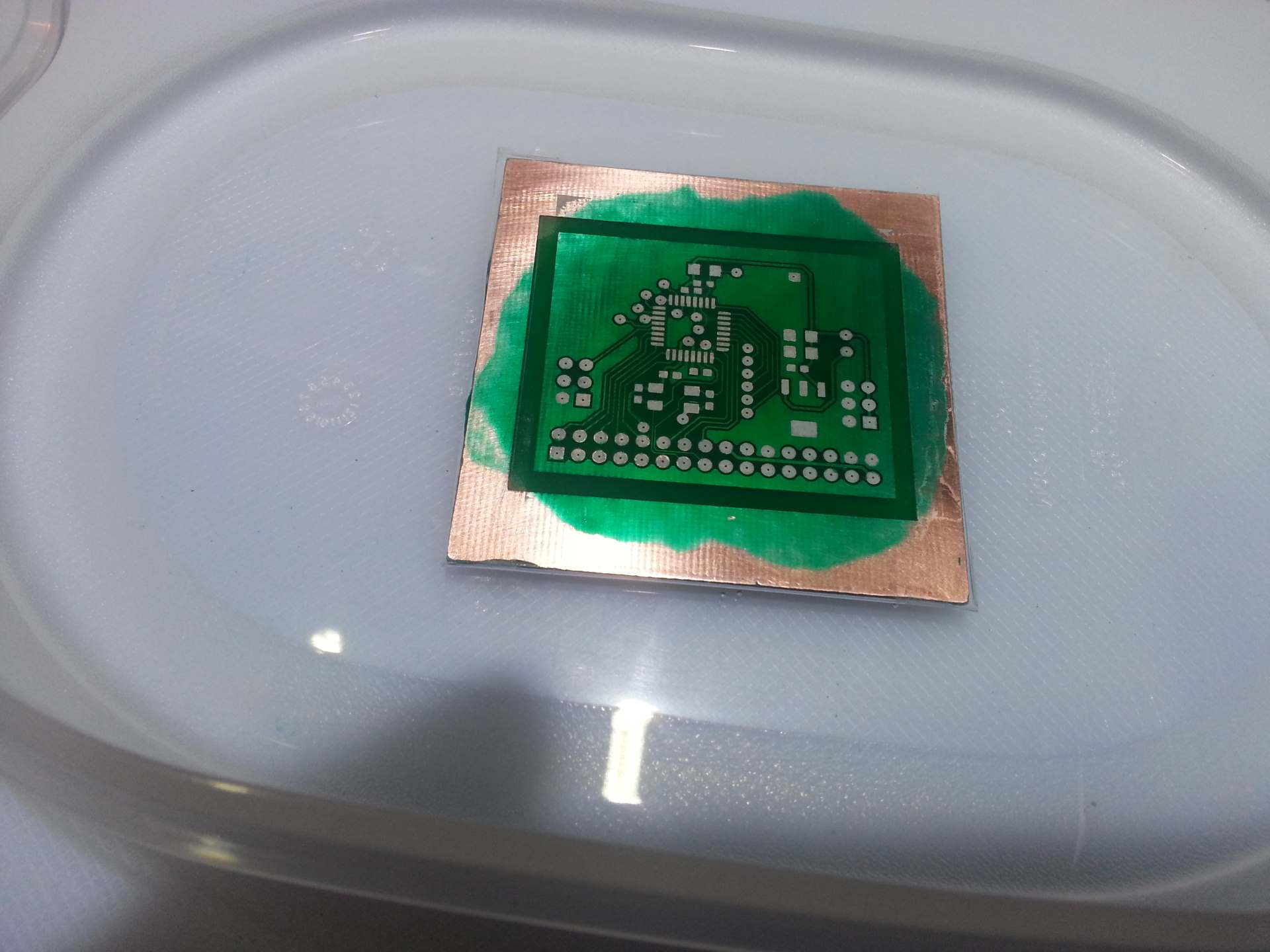
And this is the final result. My 6-mil traces are intact and conducting and none of the 5-mil clearances has shorted out. Happy happy.
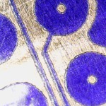
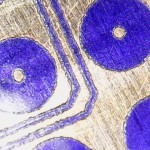
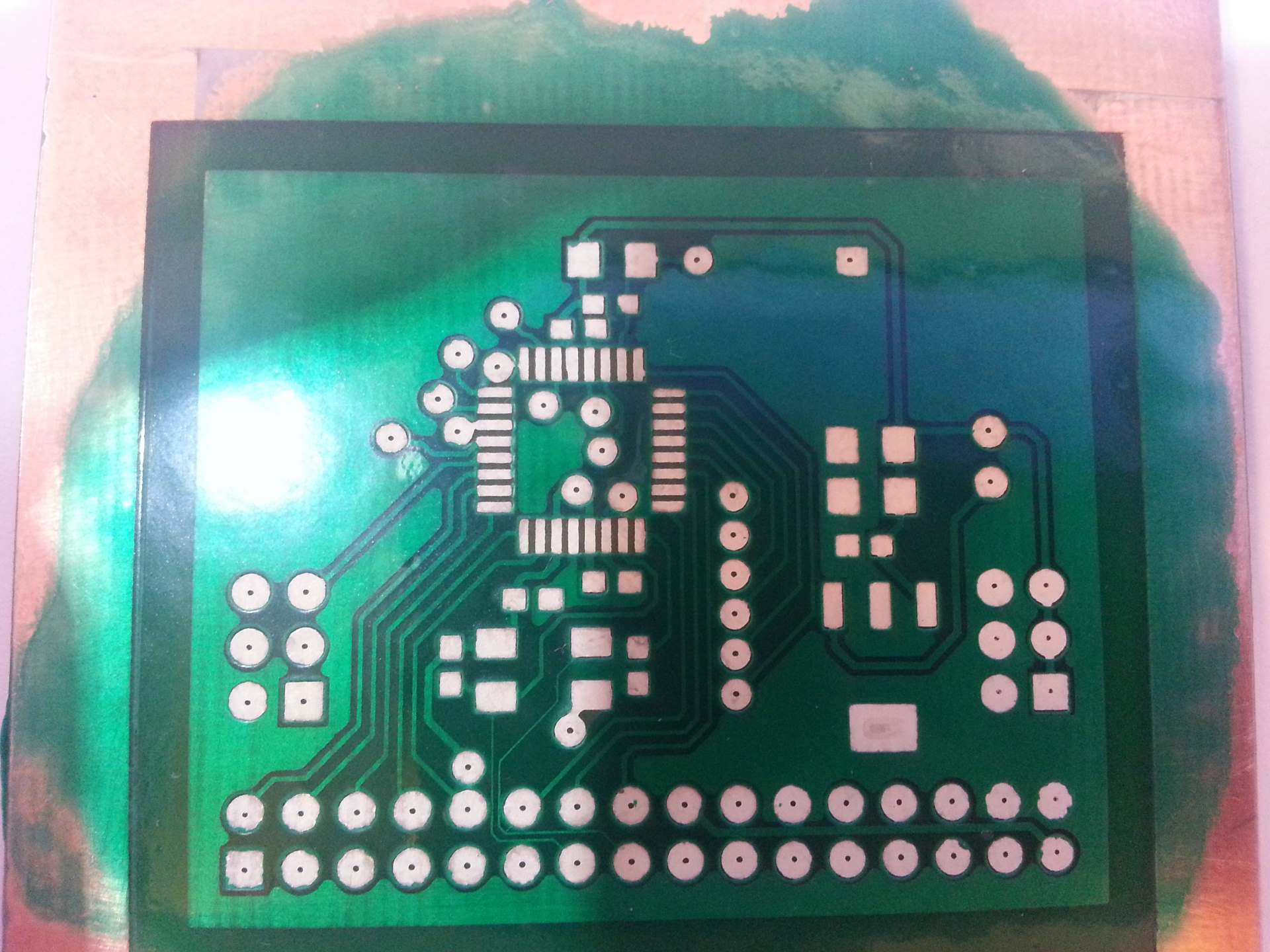
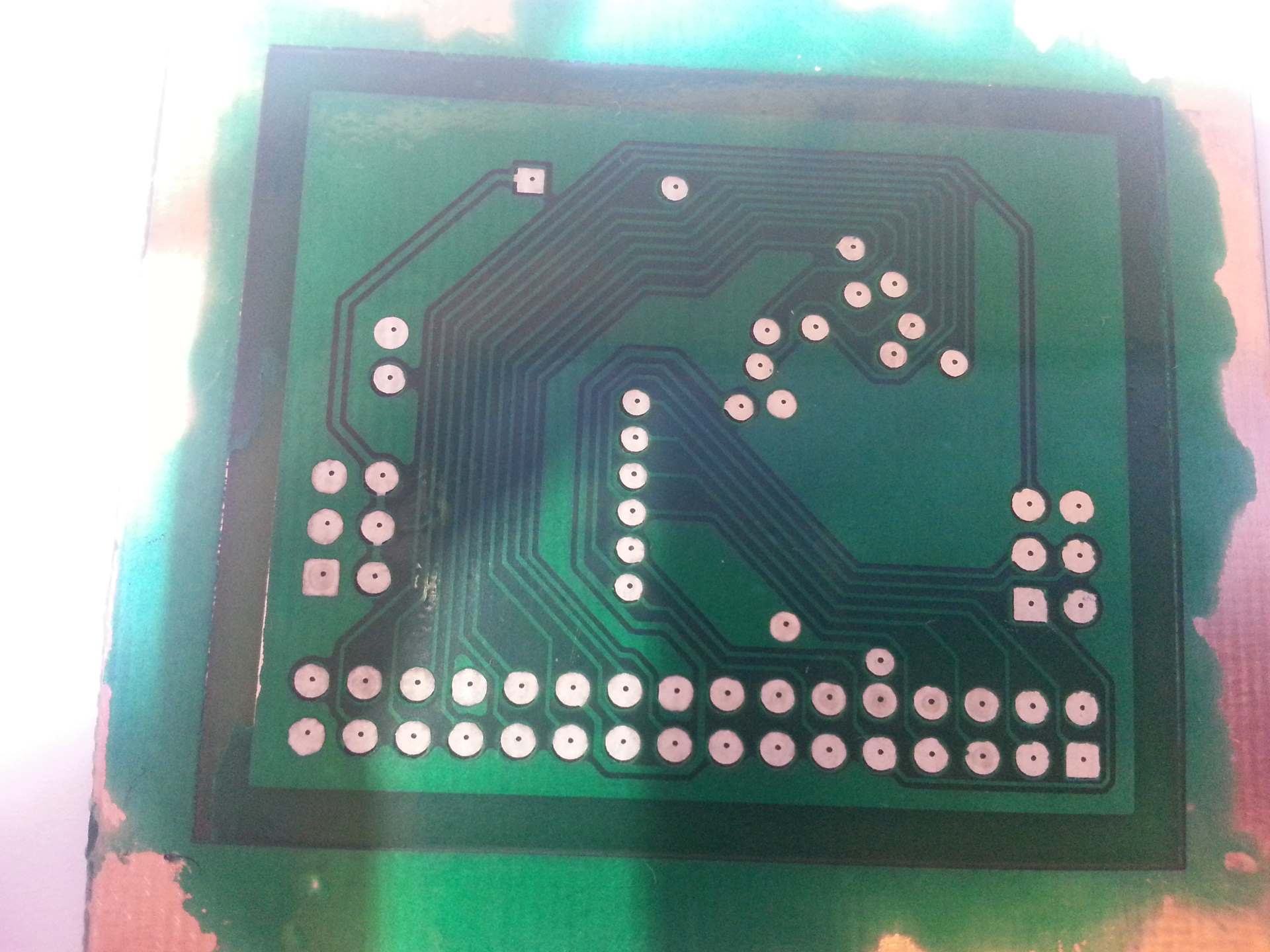
Here are some microscope images of 6-mil traces and other features on the developed etch resist:
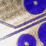
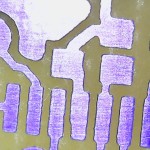
And here are some microscope images of the same traces after etching:
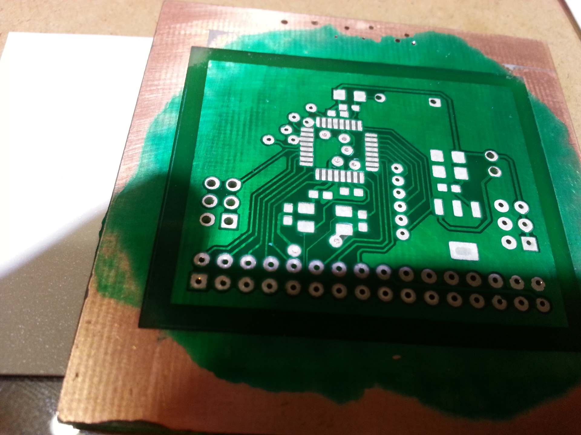
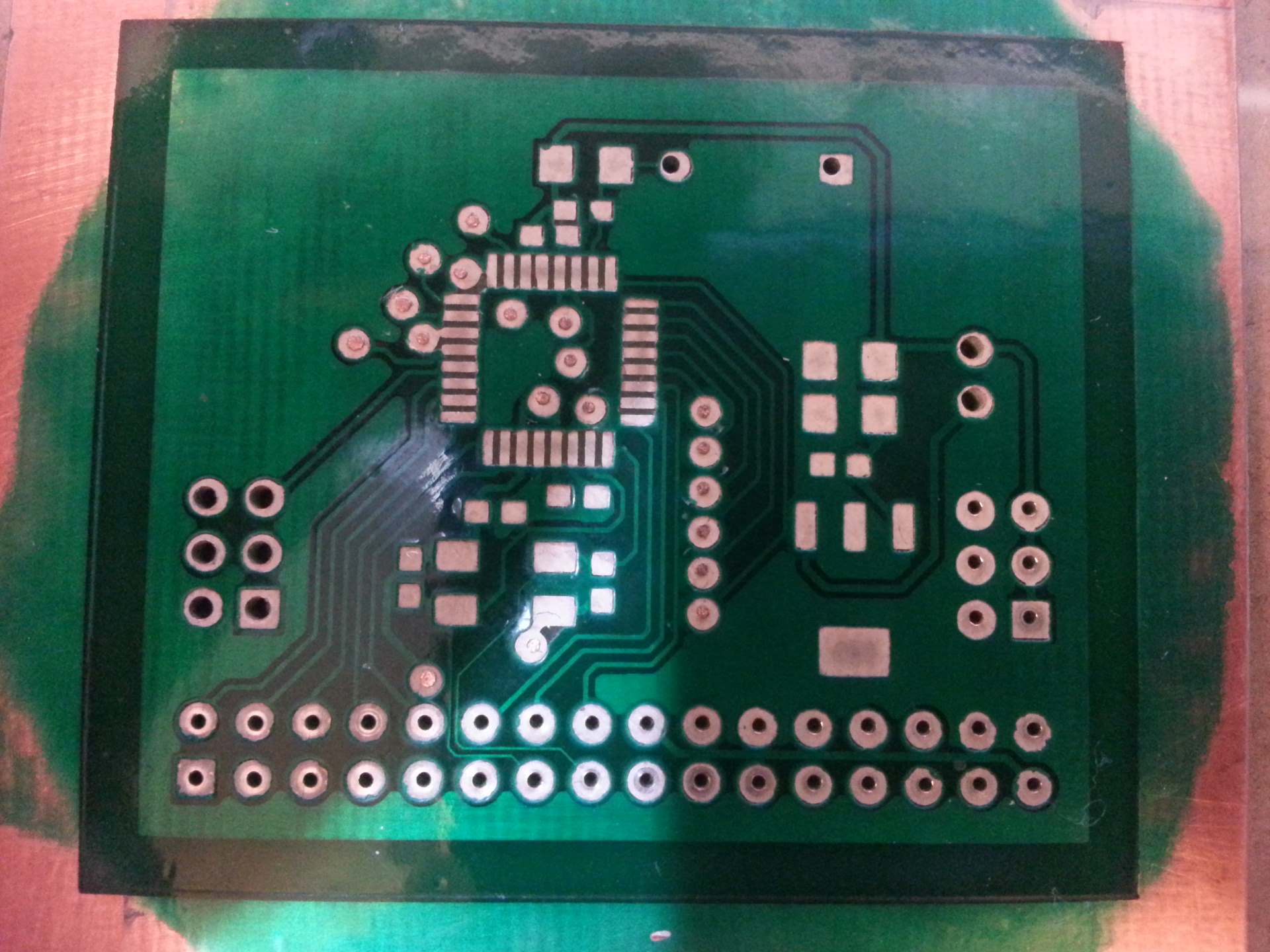
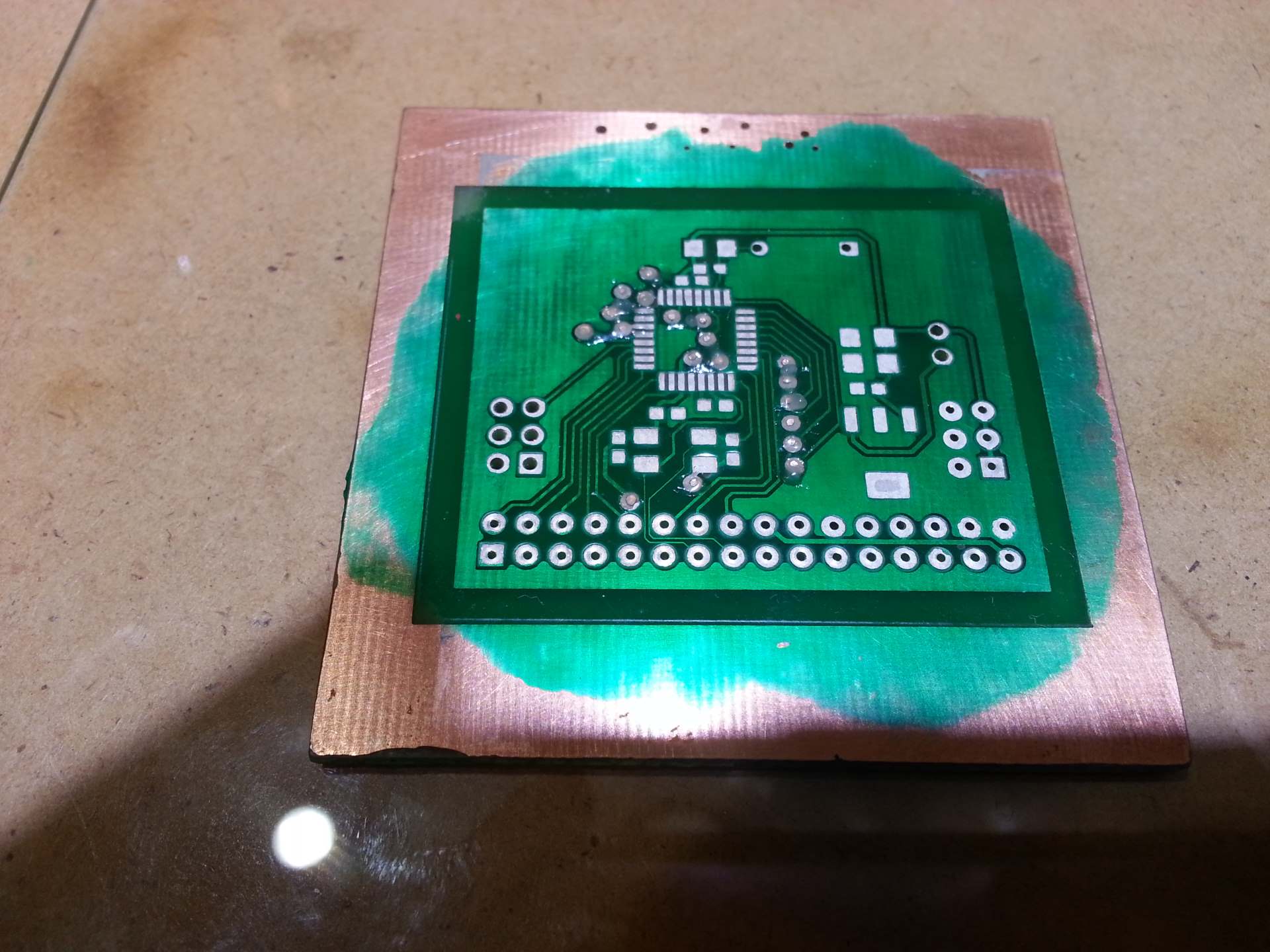
Applying solder mask
Now it is time to apply the solder mask. This is not 100% necessary, but makes soldering a bit easier, and protects the copper against corrosion. And it also give the PCB a nice look. To make the mask I apply a ~85um thick film of UV curable paint/gel and radiate it with UV through a mask like when making the solder resist. I buy the solder mask gel in 10cc syringes to make it easy to measure out the right amount.
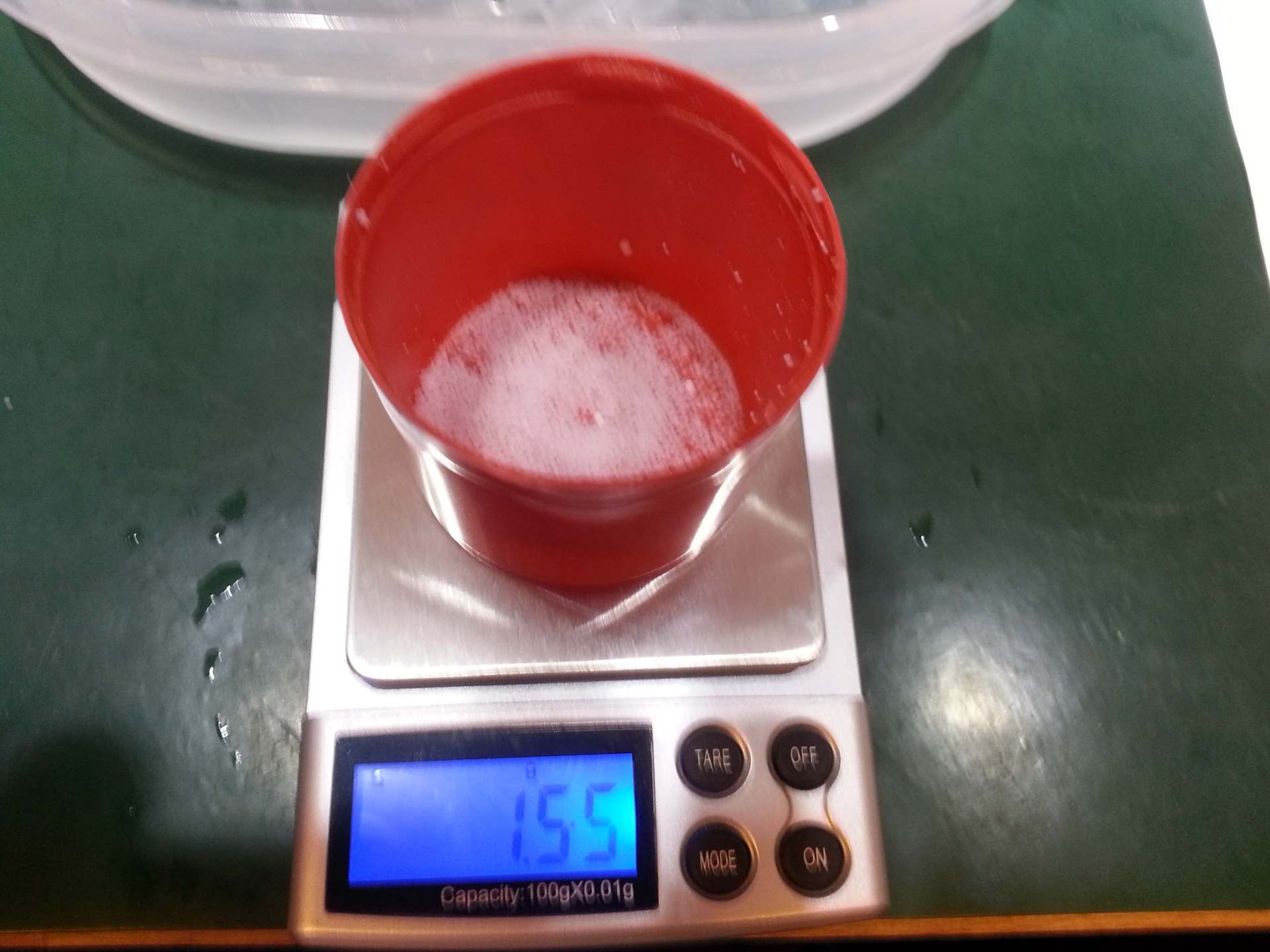
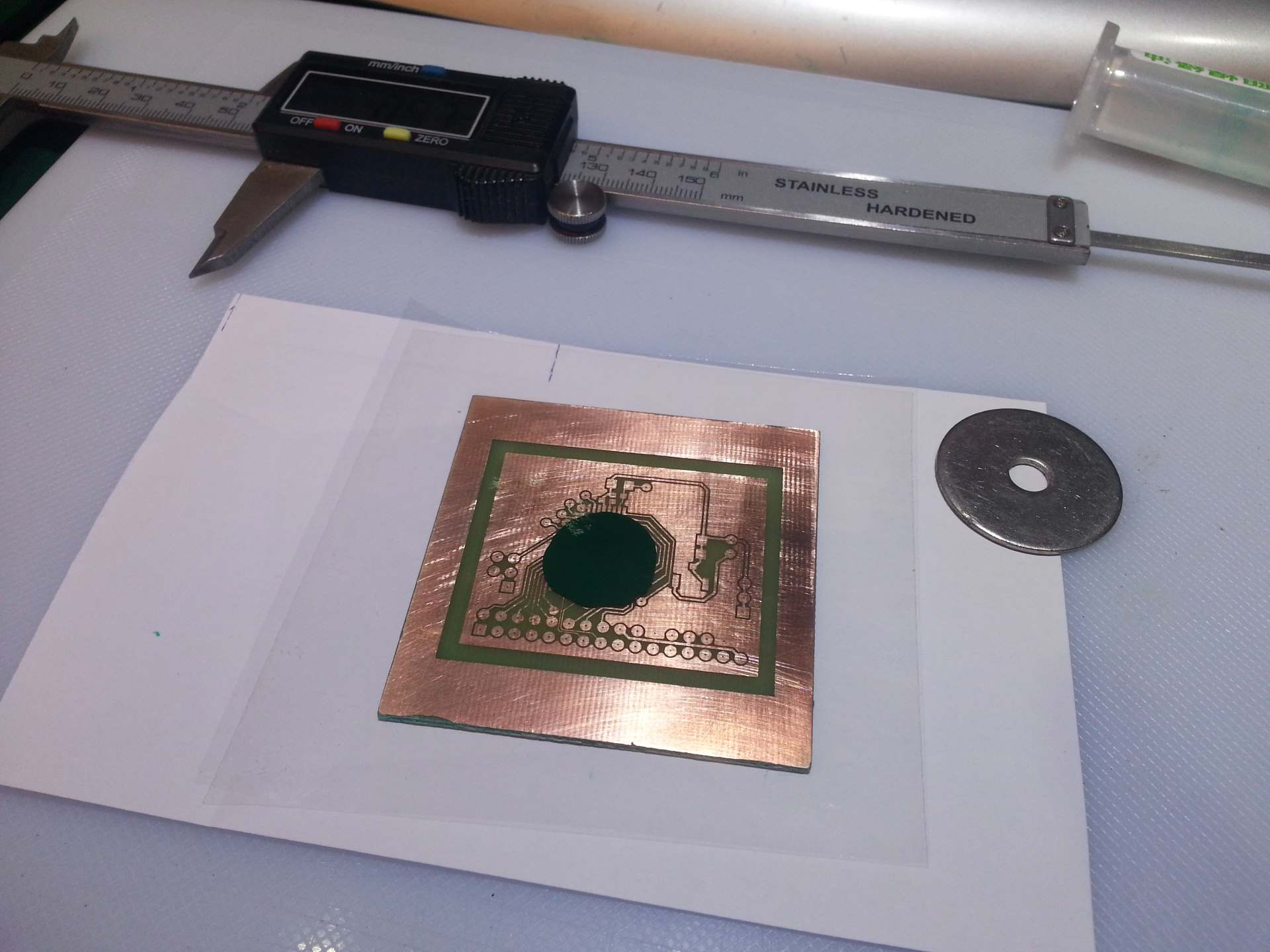
To get the right film thickness I start by calculating how many millimeters I need to push the syringe plunger to get the desired mask thickness. This PCB is 41x49mm. So I do the following calculations:
| PCB area: | 41 * 49 = 2009mm2 |
| Syringe diameter: | 15.5mm, area: π * 7.75² = 188.7mm2 |
| Thickness: | 85um |
| Volume: | 2009 * 0.085 = 170.765mm3 |
| Syringe length: | 170.765 / 188.7 = 0.905mm |
So we need to push the piston 0.9mm in to get the right amount of gel. To measure this I stick the depth gauge of a digital caliper through a big washer and let the washer rest against the syringe. Then extend the gauge until it hit the piston and press “Reset” on the caliper. Then I just need to open the caliper til it read 0.9 and use it to push the piston.
Make a pool of gel in the middle of the board and try to not get any air bubbles trapped. If there are, let it rest for a while til they float up and break.

Then I place a sheet of cellophane plastic over the gel. Again, being careful that no air is trapped. The cellophane serves several purposes. It makes it possible to spread and smooth the gel without getting any air bubbles in it. It prevent dust from sticking to the gel. It makes it possible to put the UV mask over the wet gel without messing it up. And it prevent oxygen from accessing the gel during exposure. This is important as oxygen tend to inhibit the polymerization of the gel and cause a tacky surface. Especially when using the rather long wavelength that my UV box have.
First I spread the gel roughly using a credit card. It is not super critical that it is even at this point, but it should be fairly close. Then I place the UV mask and a sheet of glass (stolen from a picture frame) over the board.
The UV mask is made from two layers of inkjet transparencies. One of the layers are mirrored and the two sheets are glued together with the ink sides facing each other. This has the drawback that we get more distance between the ink and the PCB surface. So more light can get under the edges. But since we don’t need as tight tolerances for the solder mask as with the photoreist and I use a UV box that have fairly unidirectional light, that is not causing any real problems. The advantage is that we get a much smoother surface on the solder mask. The printable side of an inkjet transparency is fairly rough, and if we press the rough side into the cellophane that rest on the wet gel the roughness will transfer to the gel.
This is also one of the reasons I don’t use tracing paper for this UV mask. The curling of the paper would cause uneven spreading of the gel. Another reason is that it is very hard to align the UV mask if it is not fully transparent. My light box is powerful, but it does not penetrate FR4 and two layers of copper!
When assembling the UV mask I only glue it in two diagonal corners. The other two corners I cut close enough that the PCB is exposed a little there. Then I place a piece of tape at each of these corners to fix the mask after the alignment is ok. The plastic masks don’t need all 4 corners to be glued in order to prevent distortion like the tracing paper masks do.
When the PCB, gel, cellophane, UV mask, and glass plate has been stacked and aligned I place the hole stack in a ziploc bag and hook it to the vacuum pump. Just like when exposing the photoresist.
I run the vacuum pump at full speed until the gel has spread evenly. You can immediately see that the dark areas lighten and the light areas darken as the pressure is applied and the gel distribute itself under the glass. When I’m happy about the “evenness” of the gel I turn the vacuum down to 70%, shut the lid on the UV box and run the upper panel at full power for 2 minutes and 15 seconds.
This is how it looks after the cellophane film has been removed. You can see that the gel is completely wet where it has been masked, and parts of it has pealed off with the film.

When the cellophane film is removed I wipe the PCB with paper soaked in acetone. This removes all the unexposed gel. This is how it looks after that.

Then I repeat the whole thing for the other side of the PCB. When both sides are done I place it back in the UV exposure box and bake it for 5 minutes with both panels at full power to make sure it is fully cured.
Tinning
After the solder mask is applied I tin the PCB using liquid tin. This is not needed it you are going to populate the board the same day, and is something I only started doing quite recently. But after a really bad experience with a board that had oxidized to much before soldering I hunted down some chemical tin and started using it. The oxide layer on the pads caused major headaches when the solder paste would not wet the pads during reflow. Tinning give it a bit more shelf life.
This first pictures is taken right after the PCB was dropped in the solution.
 This is after a few seconds. The exposed copper is turning silver and shiny. I tin the PCB after applying the solder mask as this greatly reduce the amount of copper that needs to be covered and makes the tin solution last much longer. I also tape over the exposed copper around the edges of the PCB with scotch tape before tinning it for the same reason.
 This is after a couple of minutes. You can see that the tin has turned more dull and at this stage no more tin will stick to it no matter how long you leave it in. Time to take it out.
This is how it looks after tinning. The liquid tin solution I fill back in a glass container that I keep in my lab-fridge. It seems to have decent shelf life even after mixing. At least when kept cold. I have only mixed one batch so far, and that was 4 months ago. And it still works fine.
Drilling
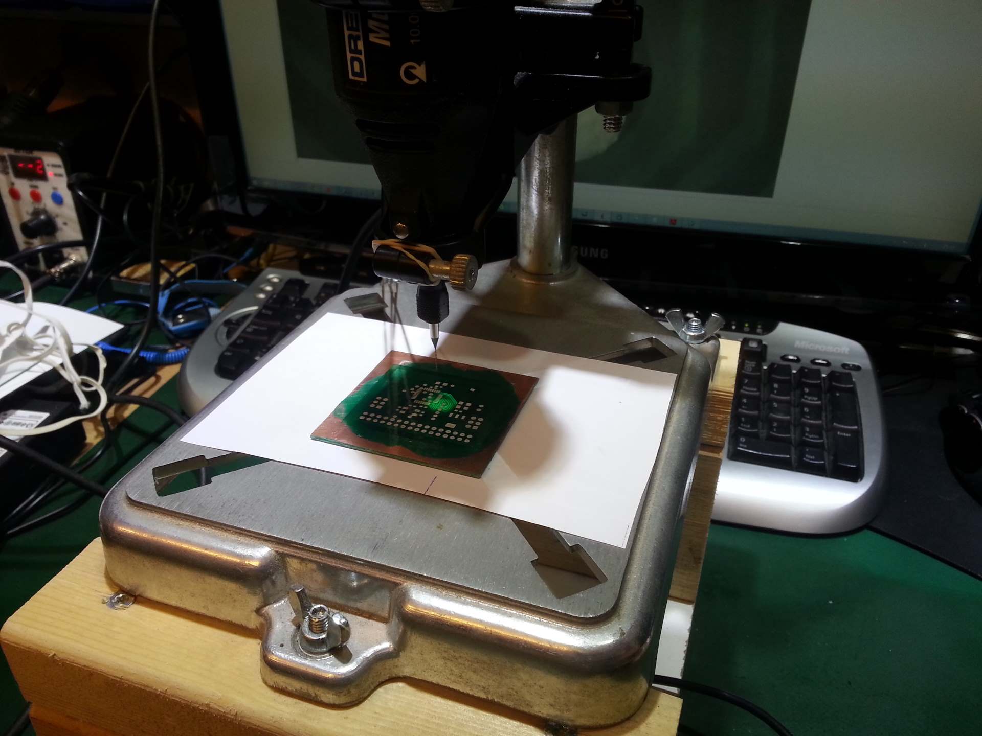 Drilling used to be the part of this job that I dreaded the most. I found it very hard to aim properly in both axis when using a drill stand alone. So I ended up building a camera guided drill jig to make the aiming easier. And now drilling is no problem at all.
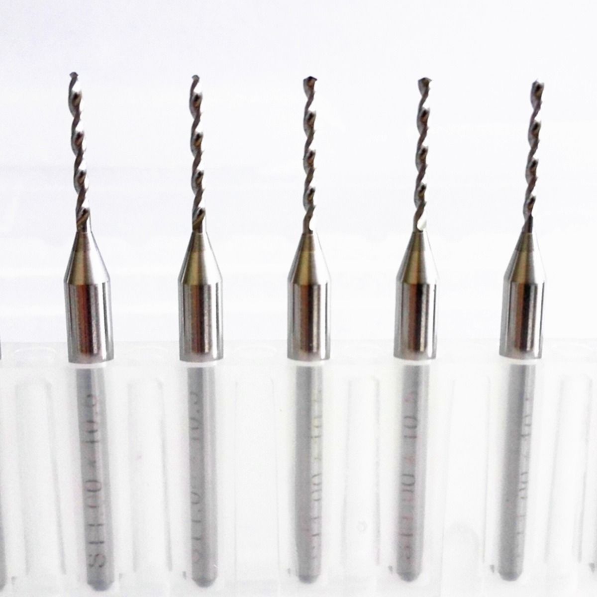 I have a large set of carbide steel bits that I use when drilling PCBs. I have sizes from 0.4mm up to 3.0mm. They can be bough very cheap on eBay and works great. Do not try to drill PCBs with reqular HSS bits. You will only be able to drill very few holes before it has been worn enough to start tearing rather than cutting the board. I tried it once, and then the bit was so worn by the end of the first board that I could not see through the last holes I had drilled. It had torn so much glass fibers out of the FR4 that it refilled the hole.
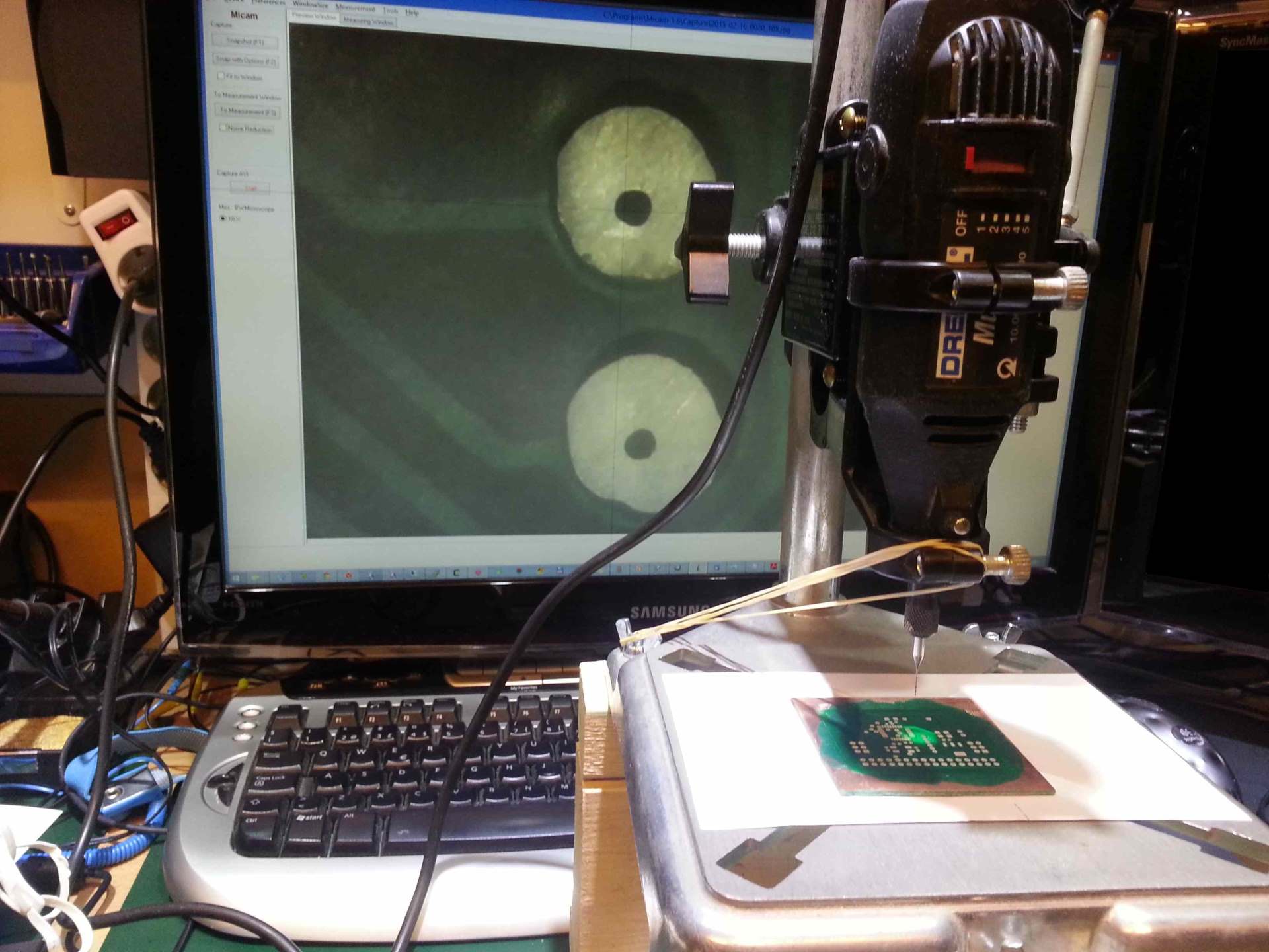 Here you can see the drill jig and the monitor with the camera image in the back. If you look at the larger versions of the image you can see a faint crosshair in the image.
This crosshair can be moved with mouse and is what I use for targeting. Each time I start up the drill I will first drill a hole in the edge of the board (the part that will be cut away in the end) and place the crosshair in the center of the hole. Now the jig is calibrated. Then I slide the PCB around and center the etched drill mark for each pad to be drilled with the current bit size under the crosshair and drill.
When all holes with the current size is done I stop the drill, replace the drill bit, and drill another hole in the edge of the board to make sure the calibration is still valid. If something has moved while replacing the bit I just re position the crosshair to make sure it is in the center of the hole again.
There is more details about how the drill jig works here.
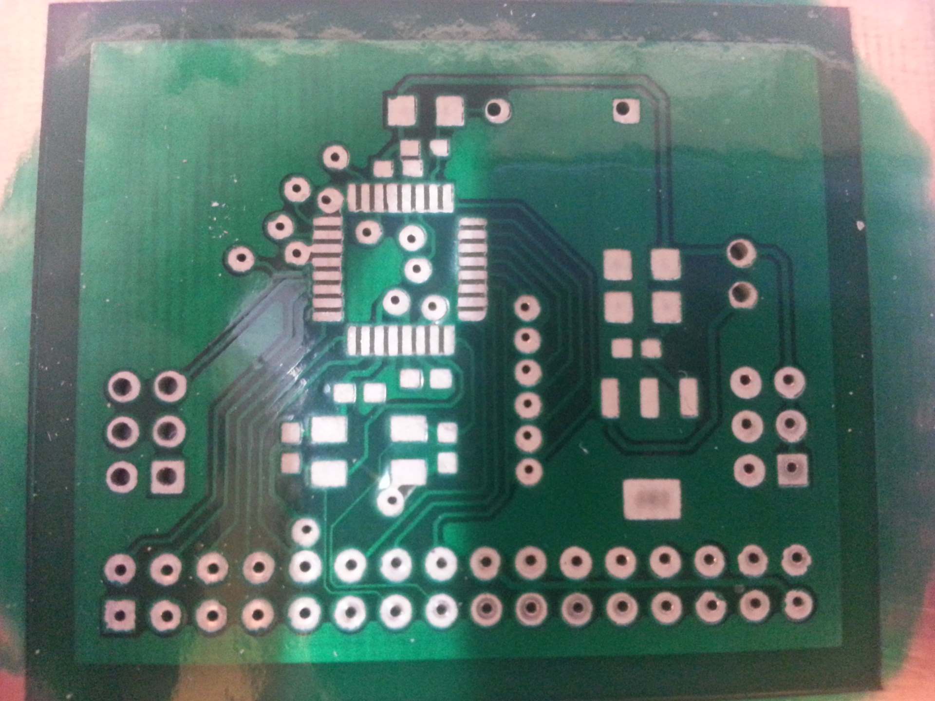
This is how it turned out in the end. The result is not perfect since the drill stand is not 100% rigid. So applying more or less side pressure when pulling the lever will cause slight variations. I hope to solve this by making it foot activated either through a bicycle-break kind of wire, or a servo motor. But it is still fairly precise and manage to always keep the hole within the pad. The variation between holes you see here is of course caused by errors in the jig and my inability to properly center the drill mark under the crosshair. But the overall tendency for all the holes to stay closer to one “corner” is because the solder mask is not 100% properly aligned. So even though the hole is well centered on the pad it looks a bit off since the hole in the solder mask is not perfectly centered on the pad.
If you plan to drill a lot of PCBs I highly recommend building something like this. I’m pretty sure I saved just about all the time it took me to build it on the first board I drilled with it.
Making vias
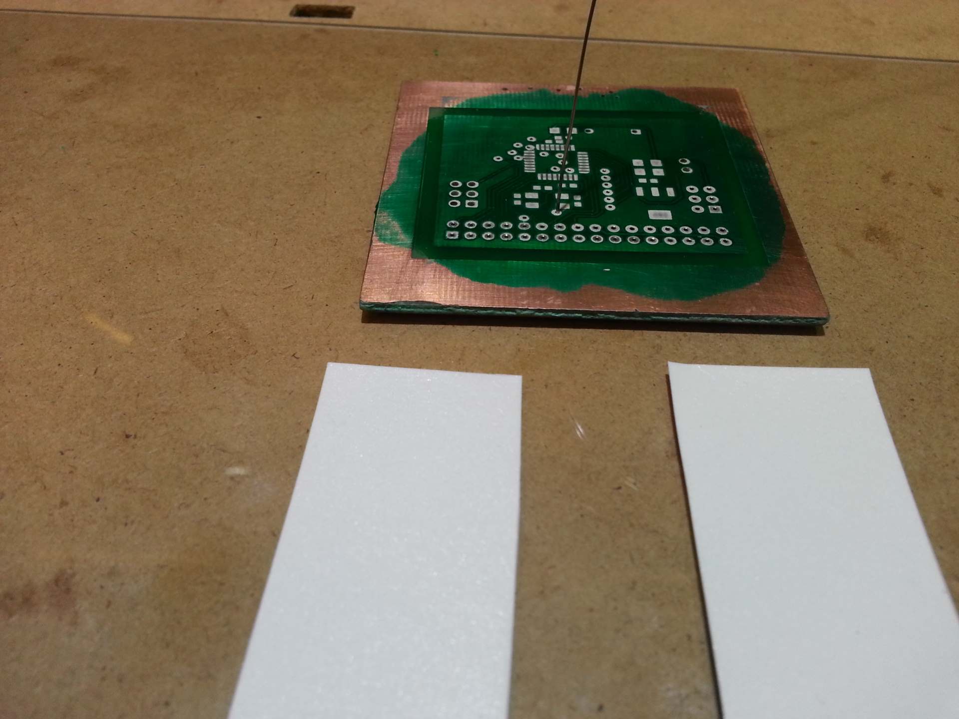
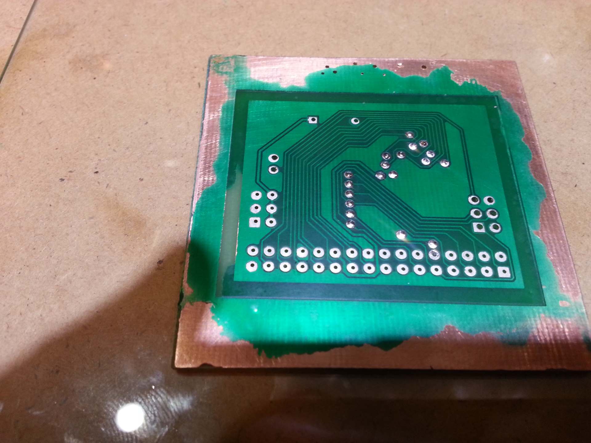
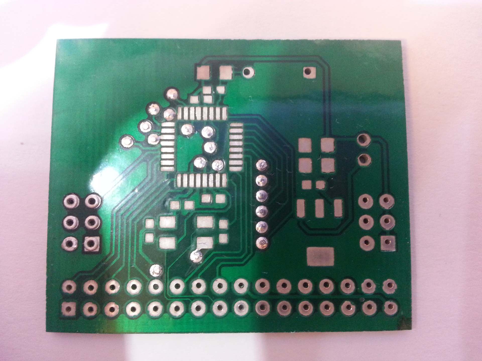
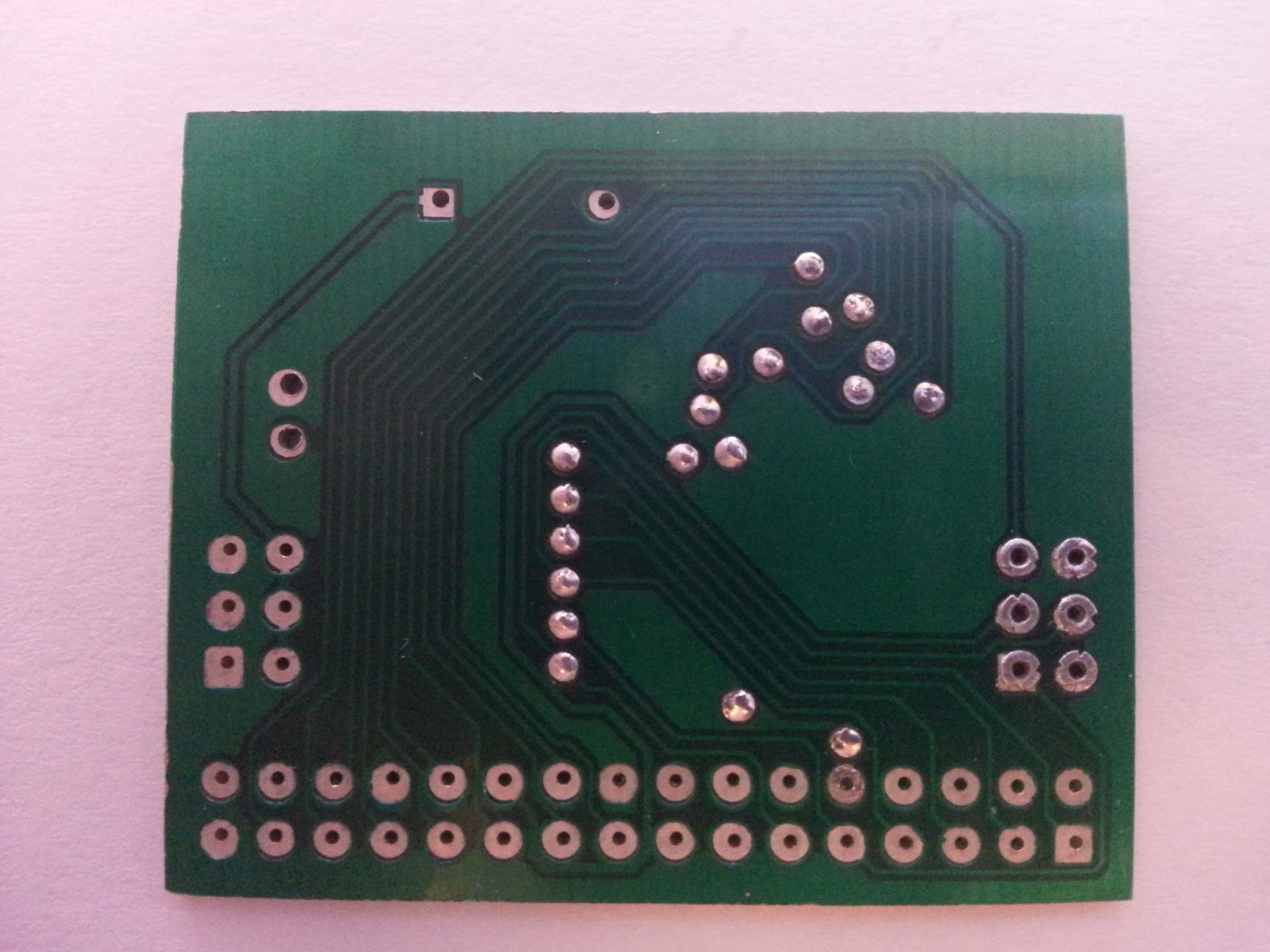
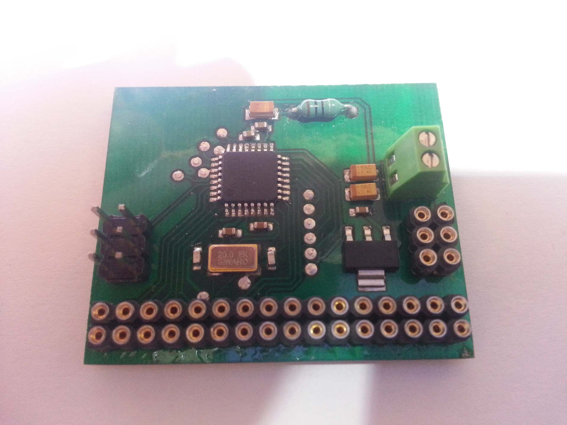
 If you make double sided PCBs you will quickly need vias. And if you need vias you will probably end up needing one under some very low profile SMD component. The PCB I’m making here have five of them right under the ATmega328 QFP-32 chip.
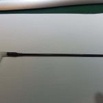
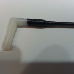
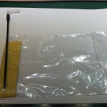
So I have found a way to make low profile vias fairly quickly. The main tools needed you can see here.
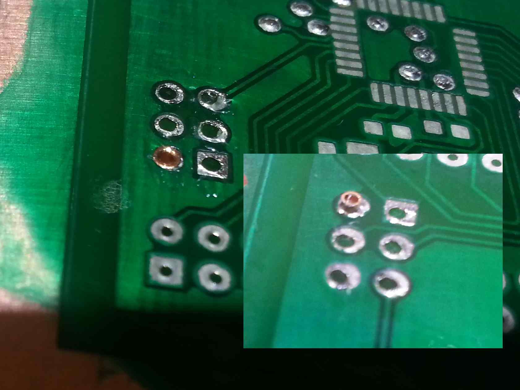
The vias are made from 0.5mm copper rivets that is soldered to each side of the board. The “head” of the rivet and the solder all fits within the thickness of the solder mask so it appears to be completely level with the board.
 The rivets are made from a 0.5mm single-strand tinned copper wire. To make sure it is straight and fit nicely in the holes I start by dragging it through a folded 1200 grit dry/wet sandpaper. I hold one end of the wire with a pair of pliers and squeeze the folded sandpaper while pulling it through. I repeat this until it is easy to make the wire enter the via holes. These holes are drilled with a 0.5mm bit to make sure they are a close fit. I now have some 0.55mm drill bits that I will try at some point. It should make the sanding step redundant and would make it easier to thread the wire. But I’m worried that it will be to much slop to make the riveting work. So until I have time to do some proper testing I stick with 0.5mm holes. I once tried 0.6mm and that was way to much. It made the wire fold up inside the hole rather than forming a rivet.
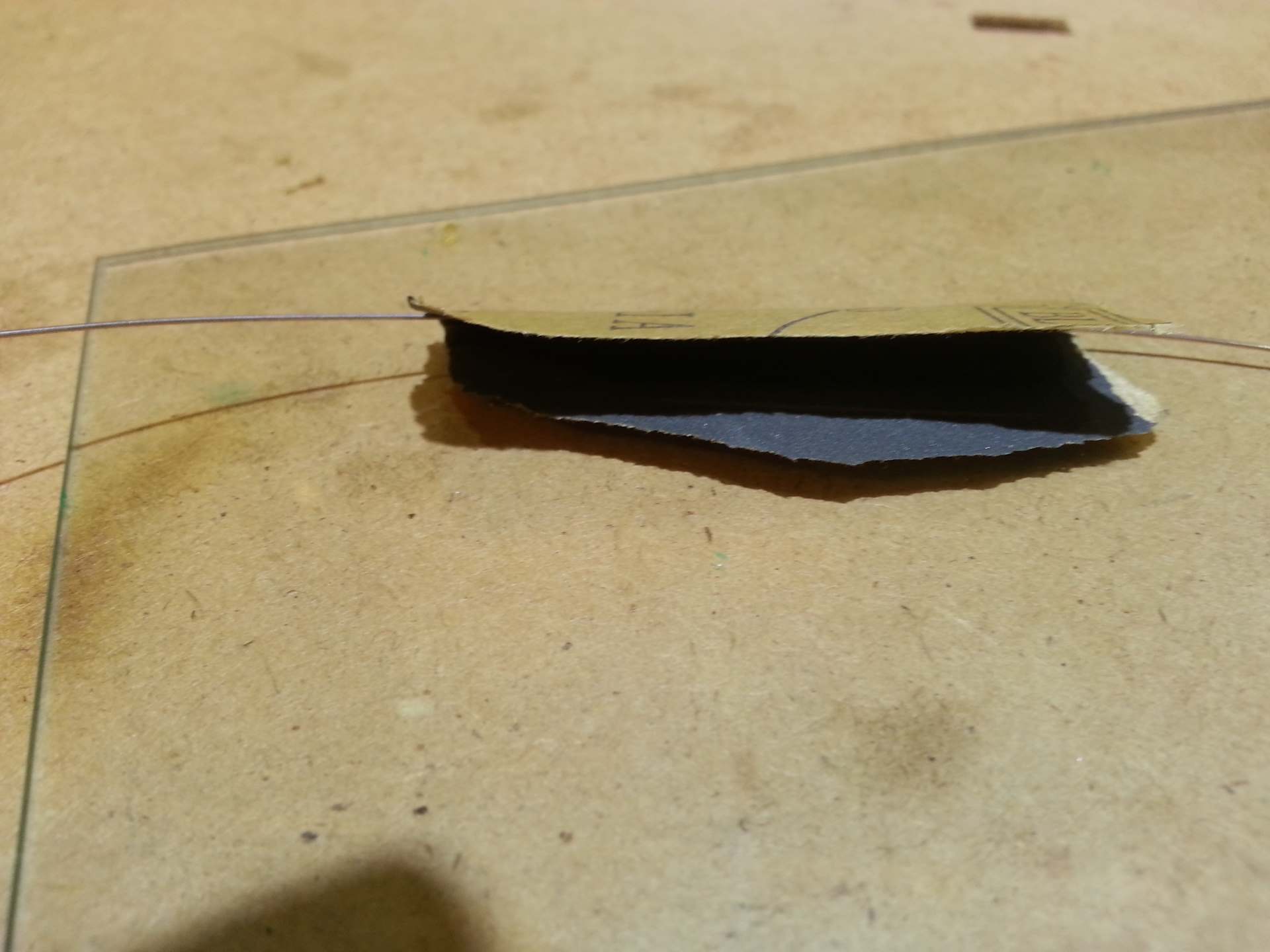
 To create the rivets I first stick the wire through the hole. Making sure it extend a millimeter or two on the back side. Then I press it back by placing the PCB on a glass plate and two pieces of thin cardboard. The ones I use here is about 0.4mm thick and that turned out to be a bit on the low side (see the microscope images at the end). But it still seems to be ok.
By pressing it towards the glass with the wire hitting between the two pieces of cardboard we make sure the wire extends a known amount on the back side.
 Then we cut the wire flush with the PCB on the front side.
 The wire now extend slightly on the back side and is level on the front side.
 Then we place a pair of locking pliers (welder’s pliers) over the rivet. The pliers has been adjusted to be fairly tight and put a lot of pressure on the rivet. Before applying full pressure we push it against the long end of the rivet to make sure it extend about the same amount on each side.

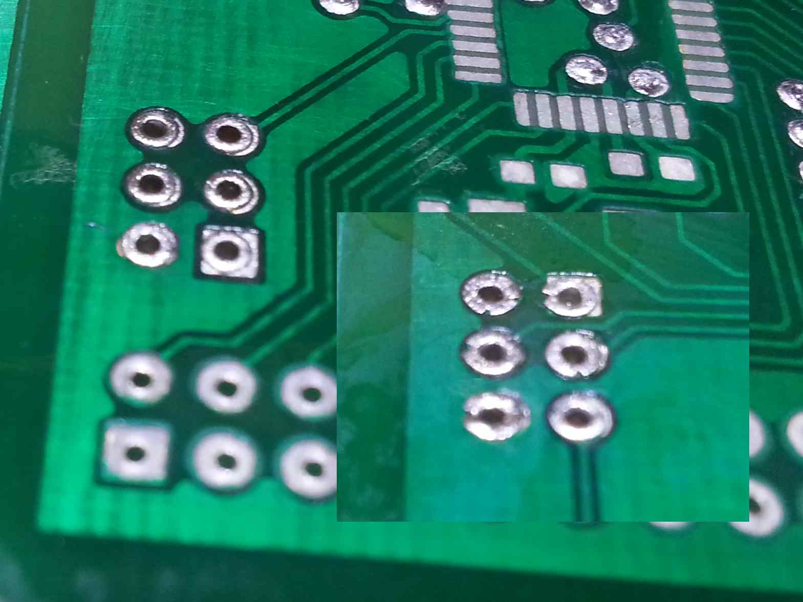
After this treatment the top of the rivet will be flush with the solder mask and are ready to be soldered.
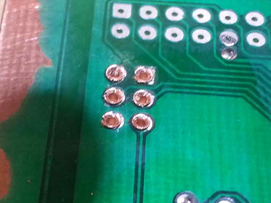
It is possible to place multiple close-by rivets and then squeeze them all together. I recommend limiting the number to 5 or so to make sure you are able to apply enough pressure to compress them all. Here I do all the 5 vias under the MCU in one go.

This is how it looks after all rivets has been placed but before soldering.
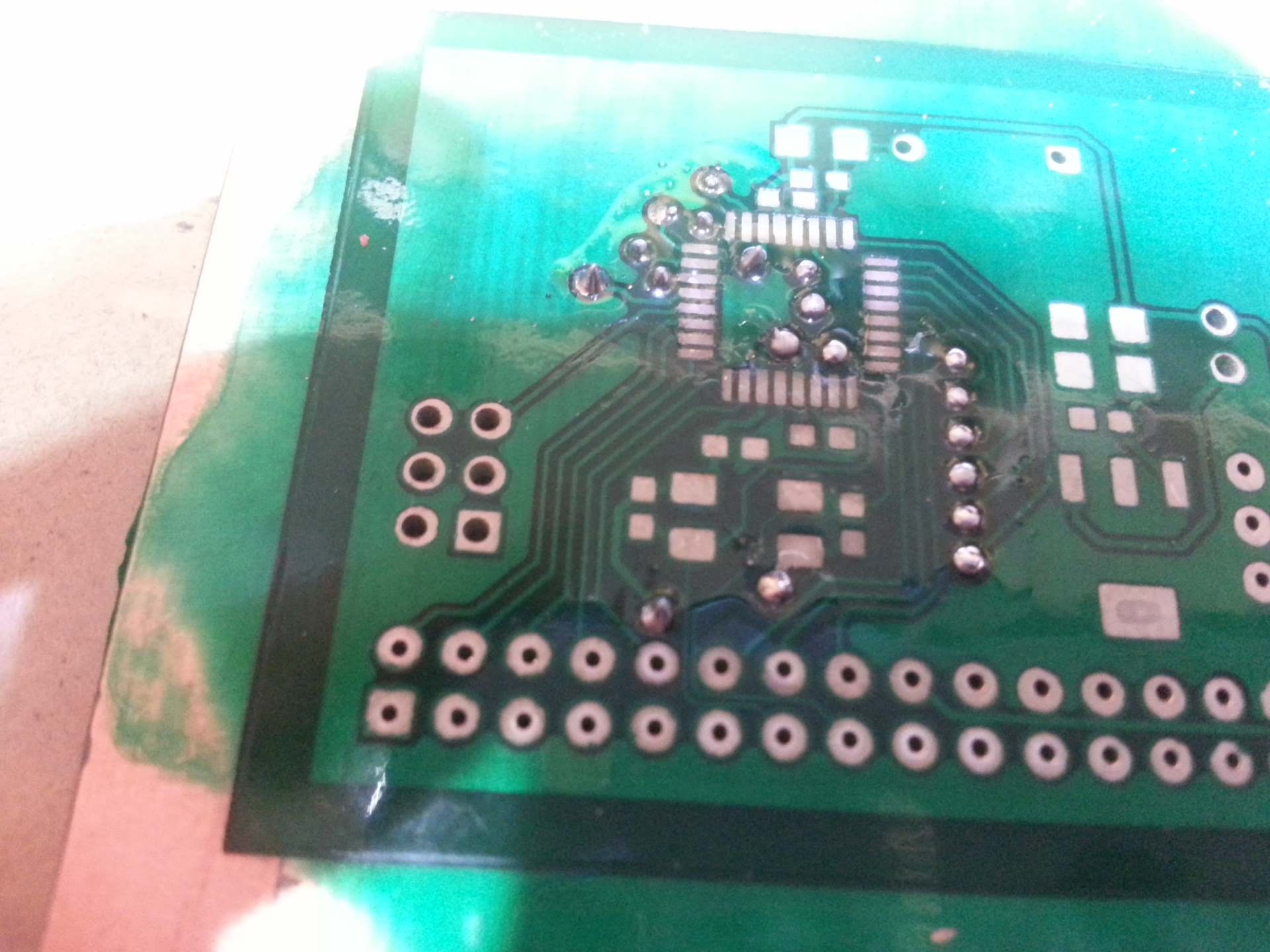
Then I cover each via with solder flux and then drown them in solder. The extra solder flux might not bee needed with a flux-core solder, but I like to be on the safe side. It is important that the solder properly wet both the rivet and the surrounding pad.

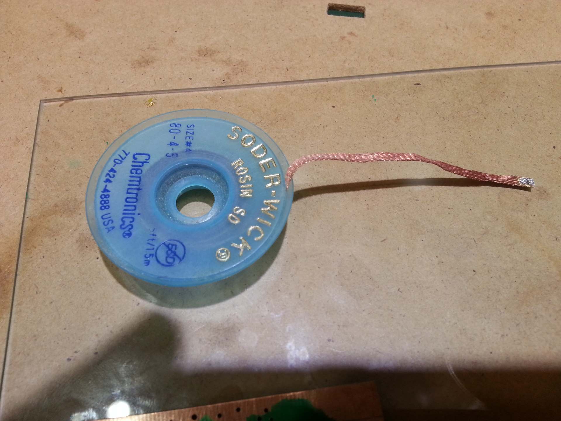
After soldering the vias are not flat anymore and they are to tall to place SMD components on top. To fix this we slide a heated solder wick over them to remove any excess solder. This picture was taken before the flux residues was cleaned off with alcohol.
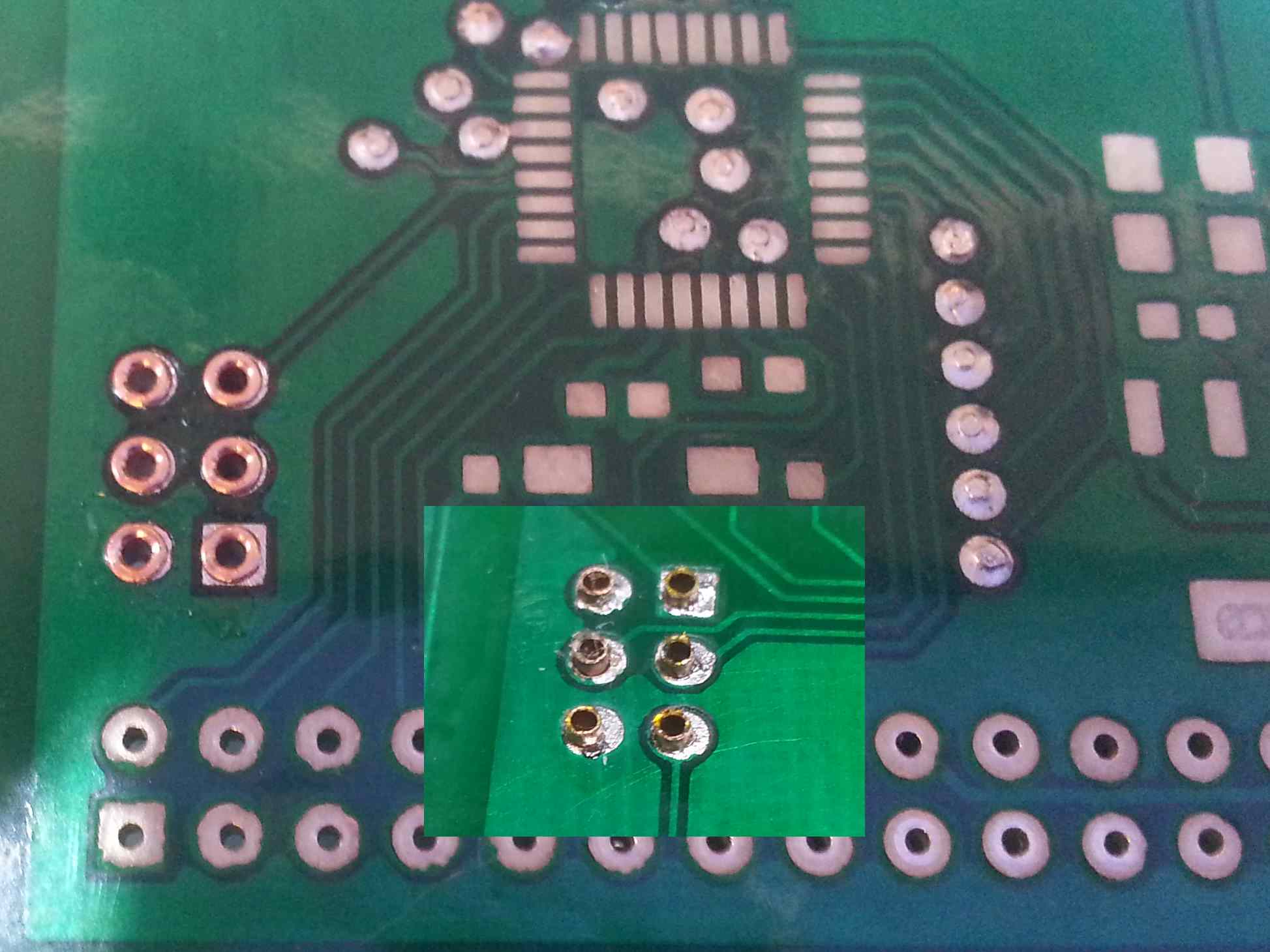
 Back side after soldering.
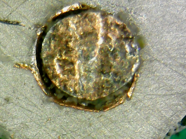
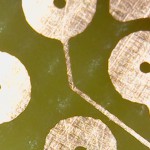
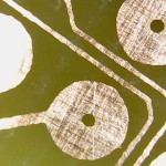
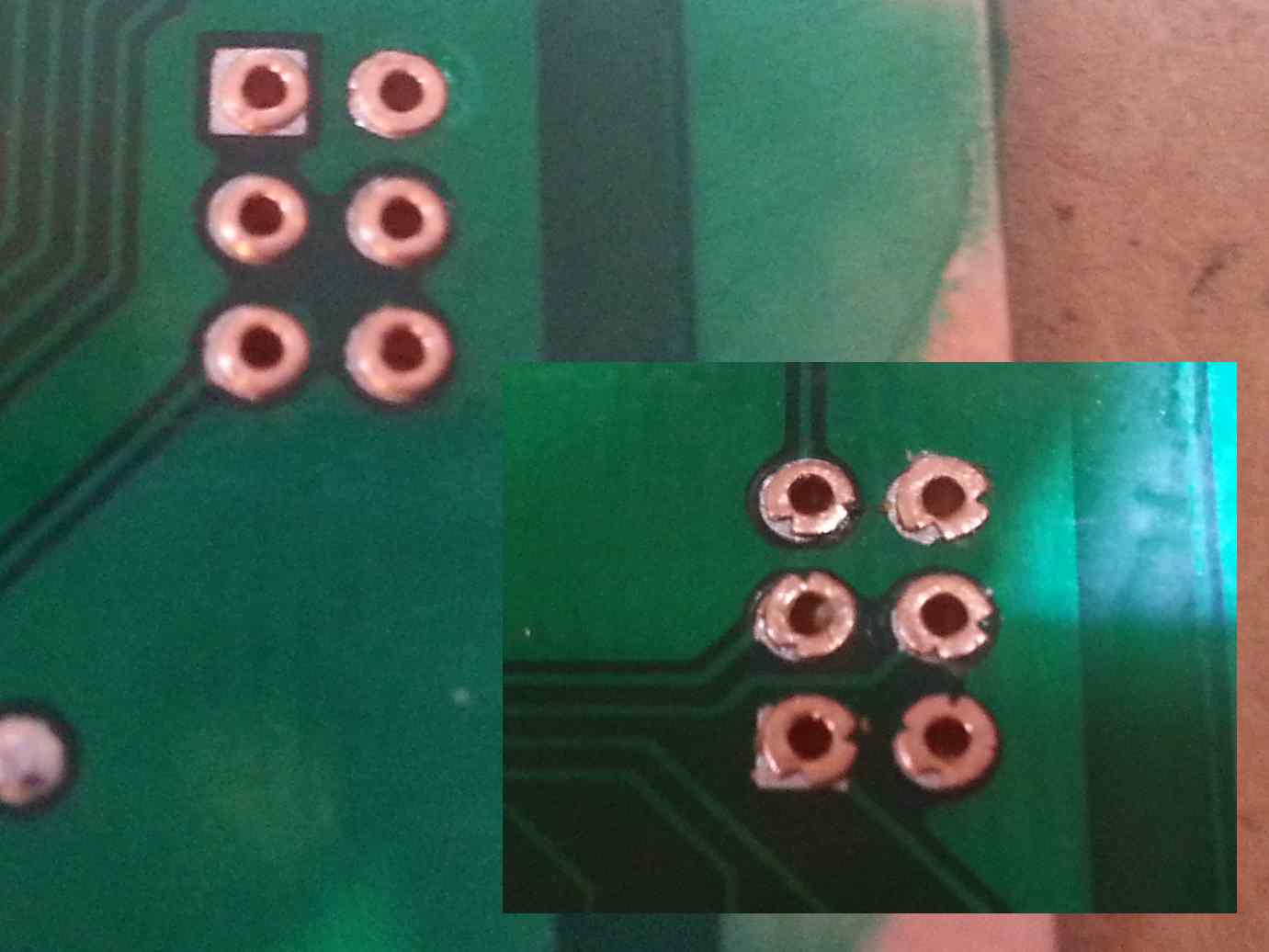
Here are some microscope images of the rivets after squeezing. You can tell that the rivets should have been a bit longer. Then they would have made more contact with the surrounding copper. Should still be fine after soldering though.
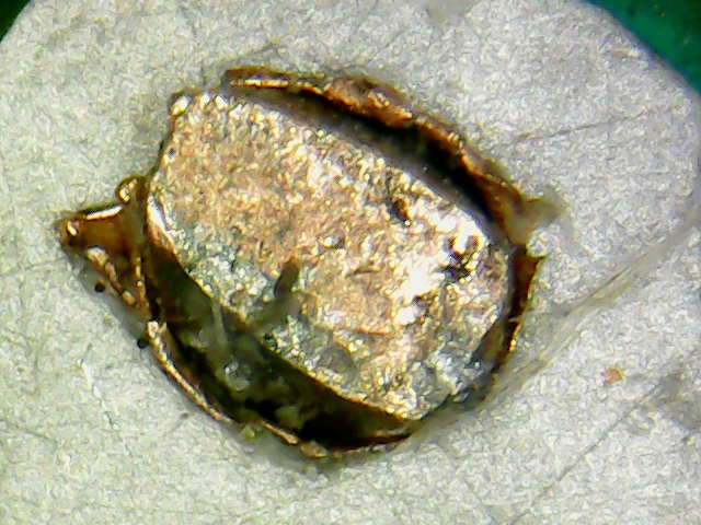
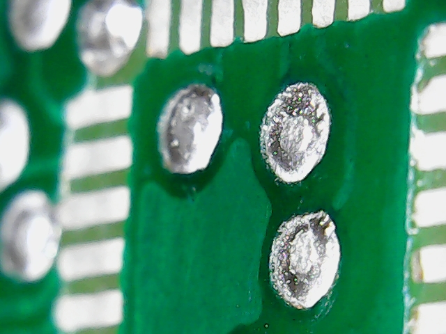 And this is how it looks under the microscope after soldering. If you look at the PCB from the edge you can see that the rivet heads fit nicely below the solder mask.
I have also made thermal vias to pull heat from an IC with a thermal pad with this vias. Then I put many vias as close as possible in a hexagon pattern and removed the whole area of the thermal pad from the solder mask. When soldering the vias I covered the whole square with a thin layer of solder. I have no real data about the thermal conductivity this give, but you are able to pack quite a bit of copper between the layers this way.
I have always been worried about the robustness of these vias though. The solder joint is probably fairly fragile, and thermal cycling might break them over time. But I have never had any of them fail. And I have some boards that are still in use and that was made like this many years ago. So either I have been lucky so far, or they might not be as fragile as I fear.
Through hole plating
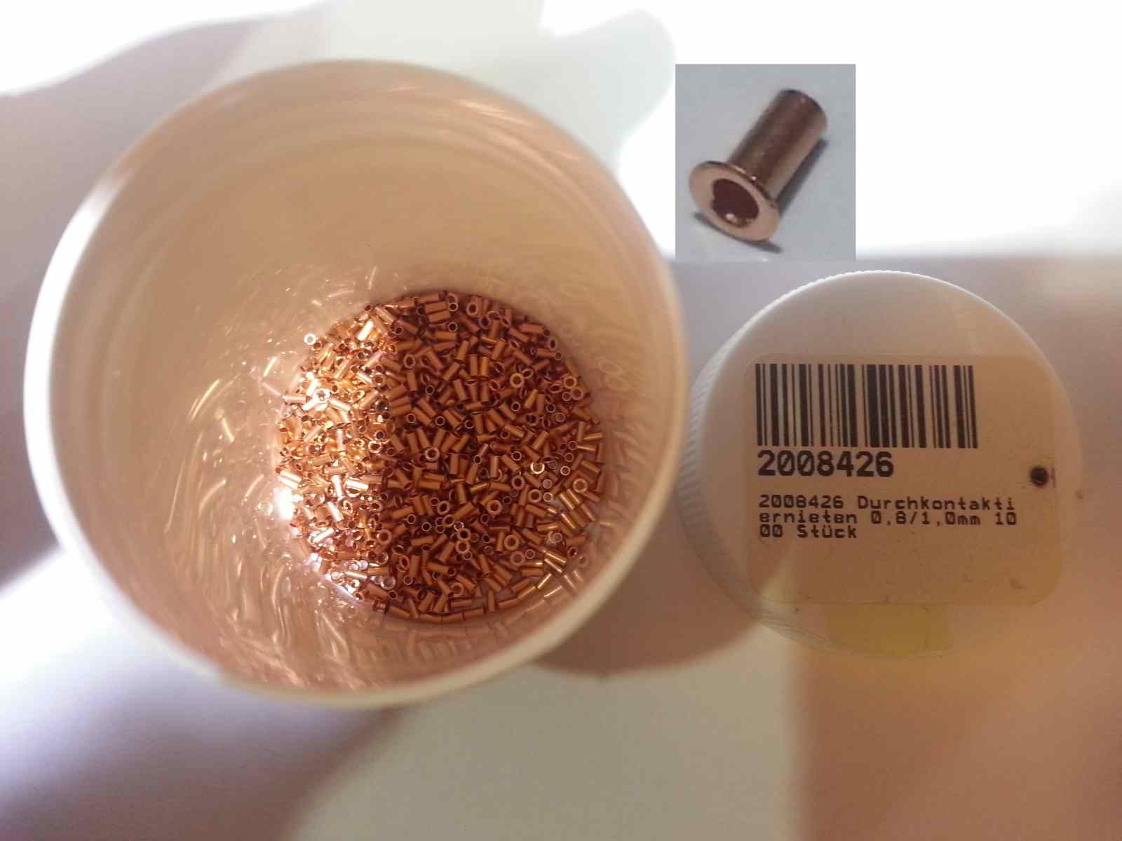 On a dual sided PCB there will often be a need for connecting a through-hole component pin to the top layer. Whenever it is reasonably easy to solder on the top of the PCB I solve it that way. But that is not always possible. Some components completely cover the top pad making soldering impossible. And then we need a plated through hole. To make those I use tiny hollow copper rivets made specially for creating PCB vias. They can be found in small quantities on eBay and in 1000-pcs boxes [here]. And probably other places as well. You can also buy a manual lever press for inserting them. And they claim that pressing them is enough. No soldering needed. But I’m to cheap to buy the press. I use a center punch and locking pliers instead. I also solder them to the pads on each side to make sure there is a good reliable connection.
 The first step is to add solder to the pads. I first add a generous amount and then wipe most of it off with a solder wick. Then I clean it with alcohol and apply a bit of solder flux.
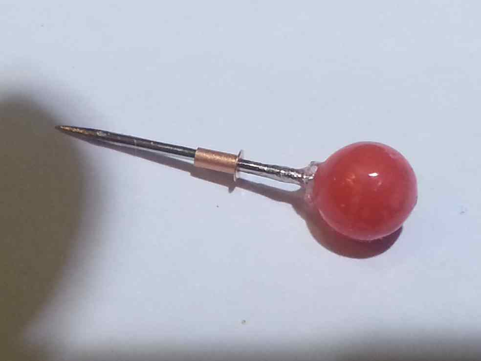 To make it easier to thread the rivets into the PCB I first thread the rivet onto a needle like this. The particular needle you see here has evidently also been used to open up a CA bottle and had a lot of dried glue on it. So that was quickly replaced before the second rivet was to be inserted as the glue made the rived stick better to the needle than the PCB.
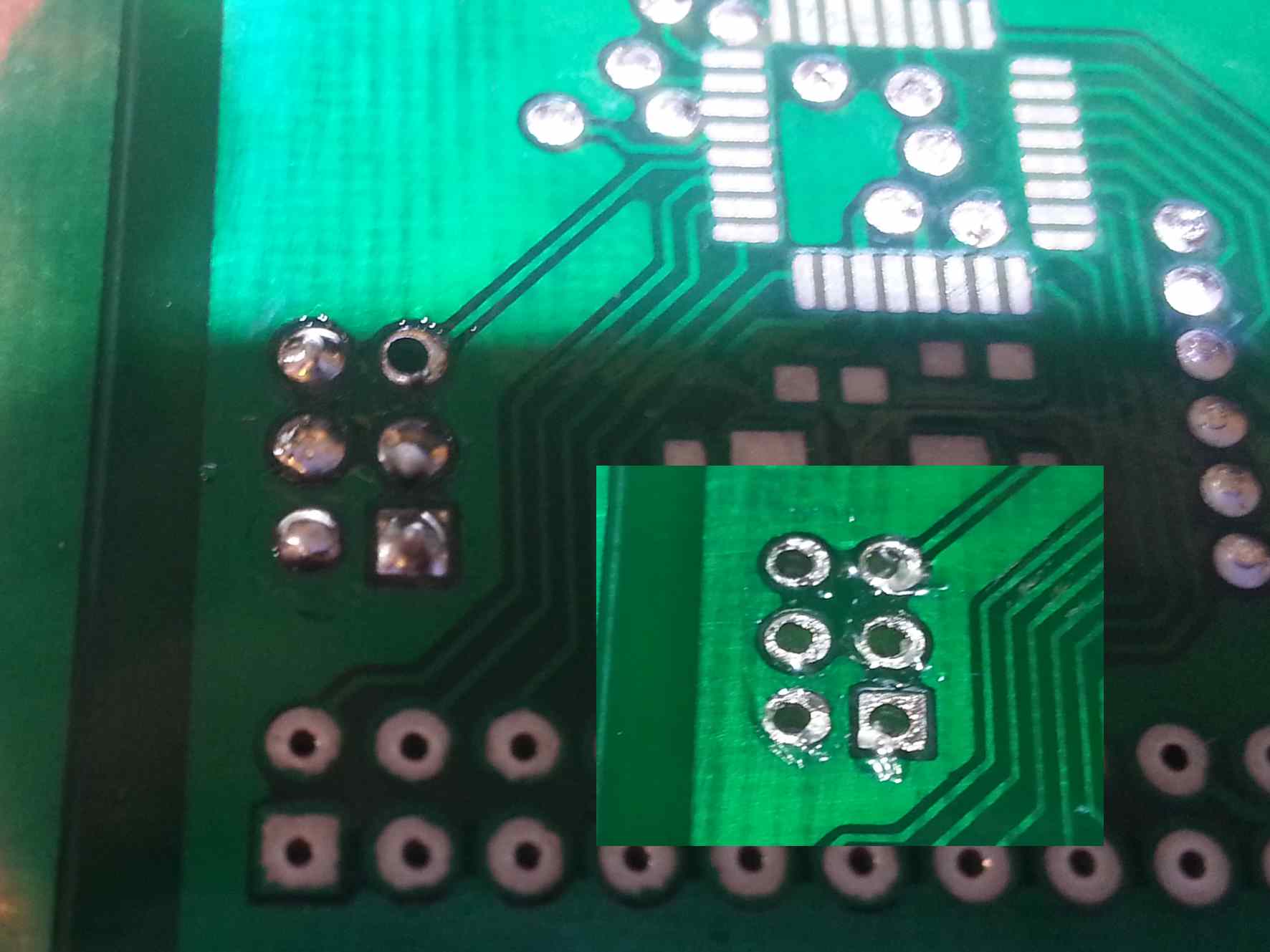
 This is how it looks after the rivet has been inserted. Top and bottom.
 And here all of them are in place.
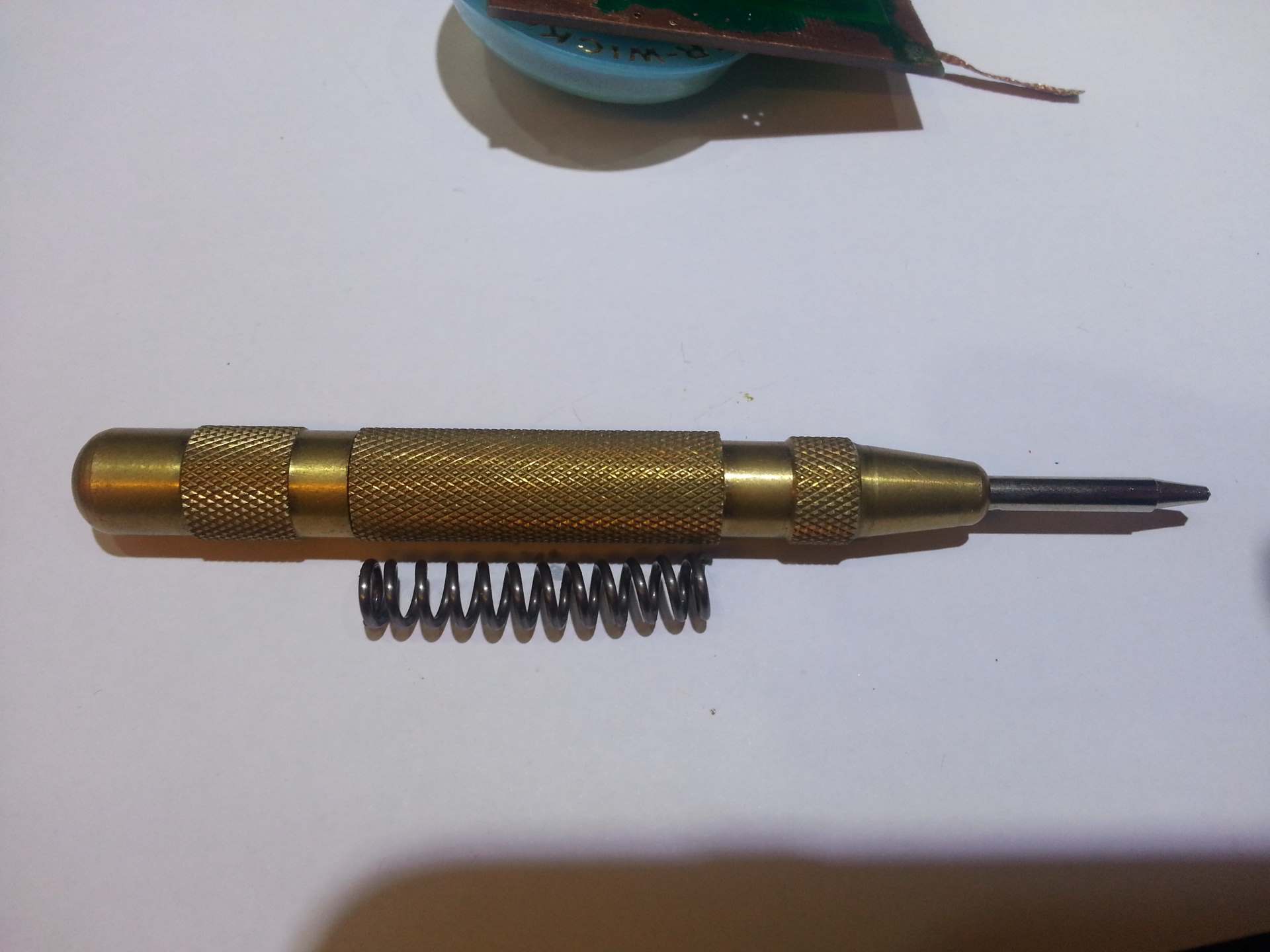 To press the rivets I start by expanding the end with a center punch. The punch I have with the best tip shape happens to be an automatic punch. And if the piston in that one activates it would punch hard enough to ruin the rivet and probably the PCB to. So I remove the back spring before using it. The rivets are very soft and just pushing it firmly with your hands will make them spread out.
 This is how it looks after being pressed with the center punch.
 When the ends of the rivets has been expanded to make sure it folds in the right direction I finish the job with the same self locking pliers that I used for the vias.
 This is how it looks after being pressed with the pliers. The top side has not changed much, but the heads are a bit flatter from the abuse.
 Finally I solder the rivets top and bottom. If the rivet head is smaller than the hole in the solder mask this will solder them to the surrounding area. And it will also reflow the solder and flux that was added to the pad before the rivets was pressed. This should hopefully assure that the hole rivet head is securely soldered to the pad.
Final cut
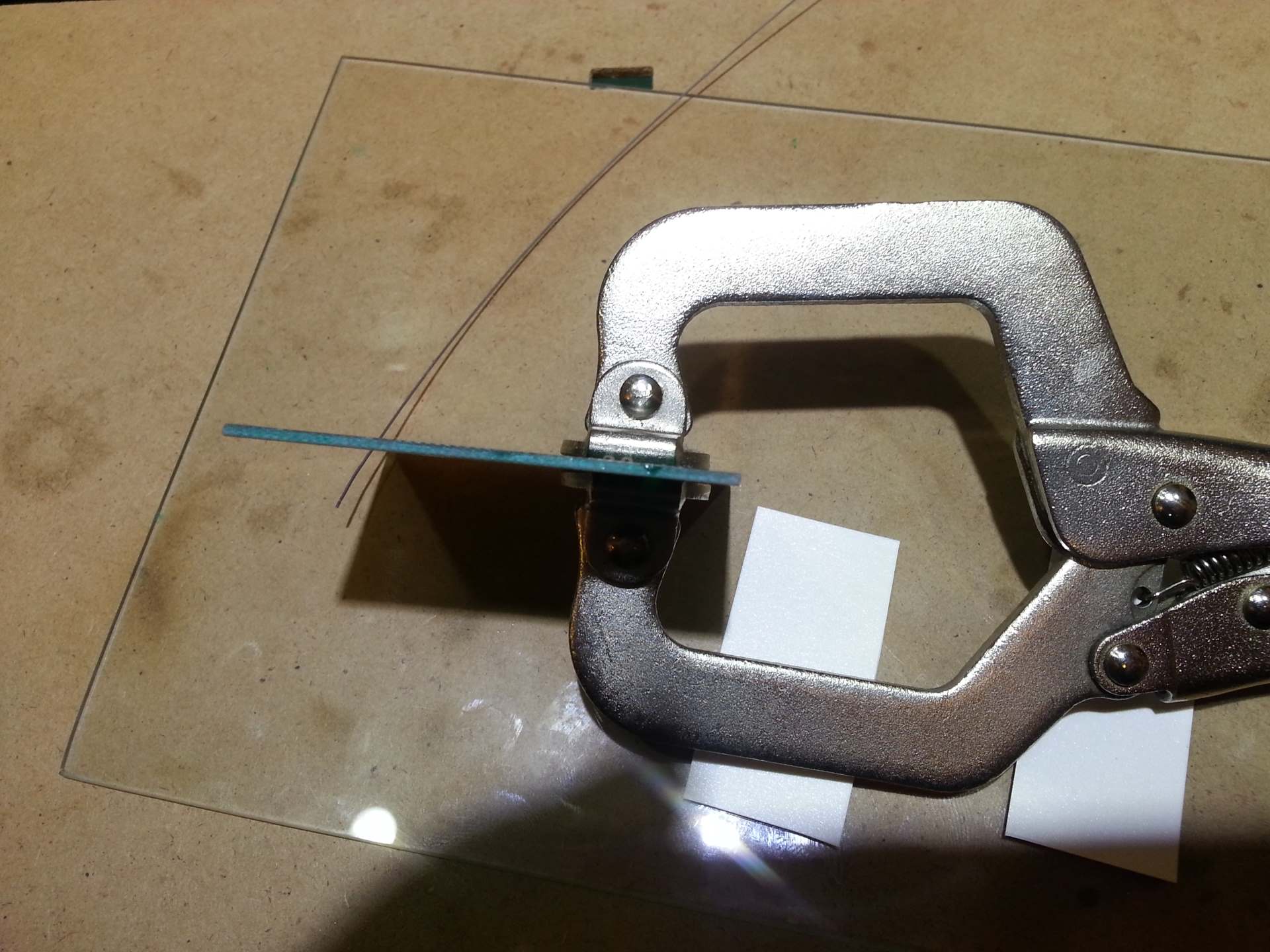
When everything else is done it is time to trim the excess off the board. To do that I use a water cooled tile saw with a diamond blade. It makes it very easy to follow the edge of the top copper fill very closely. I do not bother filling it with water though since that makes a complete mess of my workshop and is not needed at all when cutting FR4. It creates so little heat compared to the tiles the saw is designed for so air cooling is enough.
And voila! Shiny new PCB in about 70 simple steps 🙂
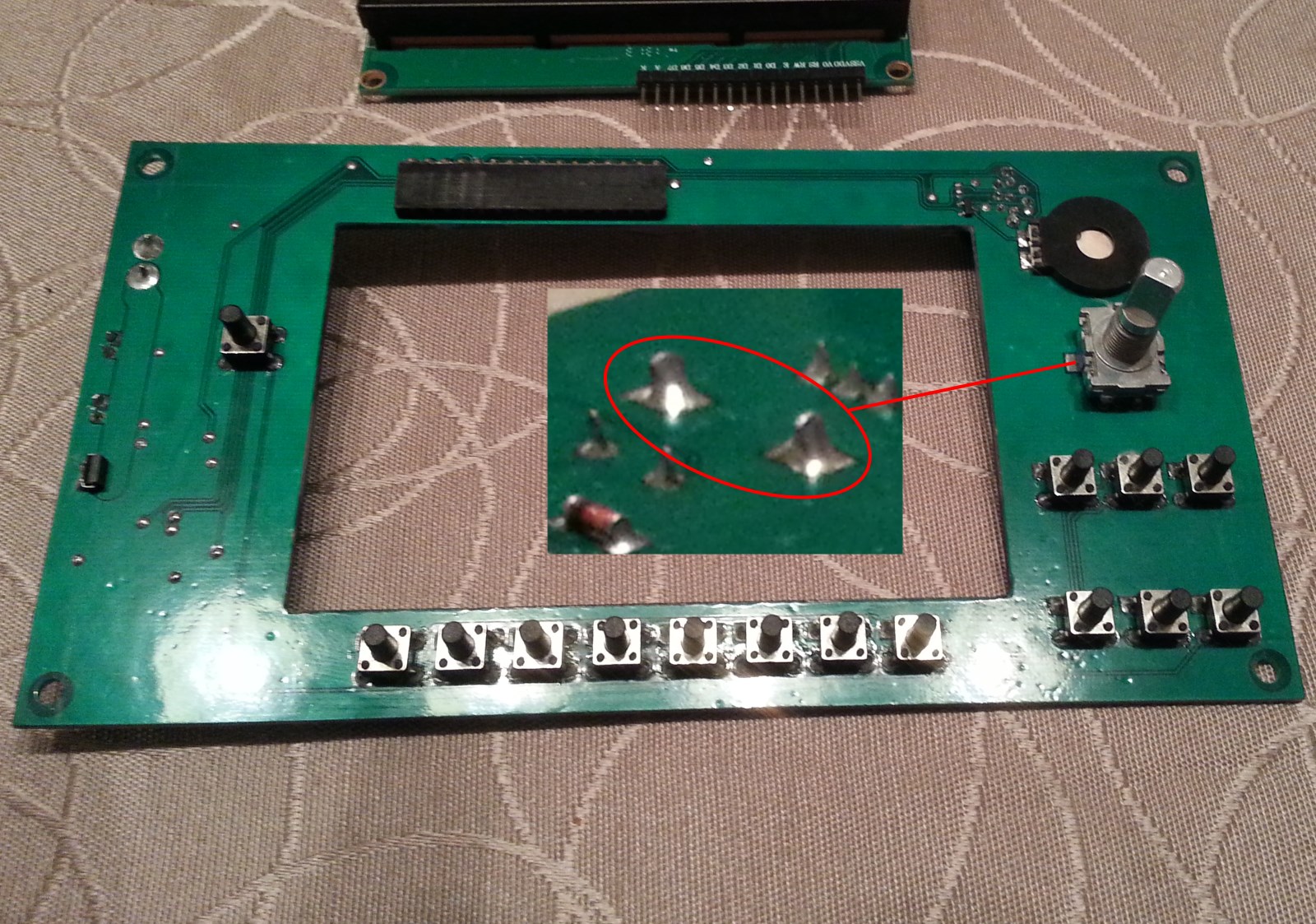 If I need to make any special cutouts in the board I use the dremel with a cutting disk for large holes and the same carbide steel drill bits I use for drilling to cut small holes.
The carbide bits work very well for machining out small oddly shaped holes in FR4. Just place it in the drill stand and lower the tip slightly into the PCB and move the PCB around to make the cut. Then lower it a little more and retrace the first cut. Repeat this until you are trough. With the thicker bits this is very easy to do. With the smaller bits (<0.8mm) you have to be really careful to not snap it. But I have used at least down to 0.6mm with no problems. Just make many shallow cuts.
The large hole in the center of the PCB in the picture was first roughly cut with a cutting disk on the dremel and then the fine trimming was done with carbide bits in the drill stand. The slits for the rotary encoder mounting tabs was cut with a 0.6mm carbide bit.
Populating and testing
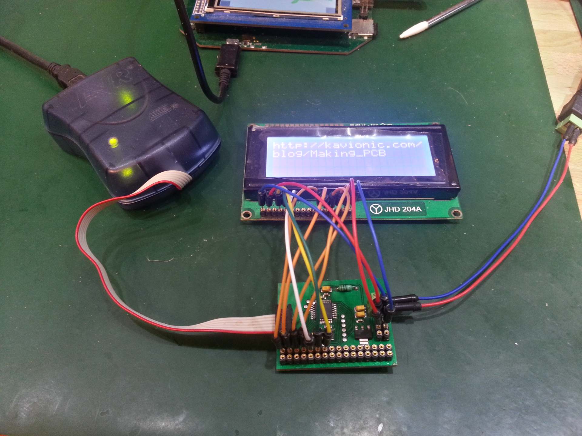
Board after assembly (left) and first test run (right).
Chemistry
Her is a list of the various chemicals I used to create the PCB.
- Developing photo resist: To develop the photo resist I mix 0.85% Sodium Carbonate (Na²CO³) with deionized water.
- Developing solder mask: To develop the solder mask I use acetone.
- Stripping: To strip the photo resist I mix 1.5% Sodium Hydroxide (NaOH) with deionized water.
- Etching: The etchant is made by mixing 200g of sodium persulfate crystals per liter of deionized water.
- Tinning: I do not know what the chemical tin is made from. But I bought it from an eBay vendor. It came in two bags that had to be mixed in water. I just followed the instructions. Except that I weighed the content of each bag and calculated how many grams I needed per ml of water. Then I used this knowledge to mix only as much as I needed to submerge a PCB in the container I use.
I always use deionized water when mixing the chemicals. Unless your tap water contains an extraordinary amount of minerals it should work fine too. I know that my tap water works fine, but I want to remove as many variables as possible. And with the small amounts I use the cost of deionized water is negligible. Besides I do not have a water tap in my workshop. So grabbing the can of deionized water save me a trip out to get it 🙂
Very impressive!
I’ve been doing a lot of basic PCBs, but I feel it’s time to take it to the next level. And your tutorial will be my guidebook.
I’m about to order some rivets for through hole plating. How long are they supposed to be? Or perhaps more importantly, how much should they protrude?
Thanks! The rivets I use are sold specifically as PCB rivets and I have not paid to much attention to their length. But the length depend slightly on their diameter. The size of the ring they produce when squished depends on how much they protrude, and the larger diameter rivets have a larger ring. This is not very critical though. I measured the 1mmOD/0.8mmID rivets and they are 2.3mm long. So 0.7mm longer than the thickness of a standard PCB (1.6mm). The 1.4mmOD/1mmID rivets are 2.7mm long. So 1.1mm longer than the board thickness. Interpolate / extrapolate as needed 🙂
Thanks a lot!
Wonderful job! If I may, I’d like plans for your UV light box and controller, I’d very much like to build it
Thanks! The project page for the UV box is here. And you can find the schematics, PCB layout, and firmware here.
There is also some sketchup CAD drawings there that should be pretty accurate, but was actually drawn as a sketchup learning exercise after I was already done building the enclosure.
Very nice tutorial! I have had so many problems making PCB’s previously. I didn’t read it thoroughly but I think that is missing how to dispose the chemicals. I wouldn’t like to throw NaOh together with the grey water.
Thanks!
Where I live it is easy to get rid of the chemicals. Just bottle it up and go to the closest garbage depot and leave it in their “dangerous materials” section. Which is free. Other countries, and maybe even other parts of my country probably have different routines for this though.
That being said, I would not worry about Na²CO³ or NaOH. The Na²CO³ I use are sold as a cleaning agent, and the NaOH are sold as a clogged pipe opener. So both are meant to go down the drain 🙂 Still probably a good idea to dispose it off properly after having dissolved photo resist or solder mask in it.
The etchant full of copper sulfate should not go down the drain. Try to find a depot for dangerous chemicals where you can get rid of that.
”
”
I do not agree. Read
https://retromaster.wordpress.com/pcb-making/
I envy your CNC drill 🙂 But I will never do TT again. I have made many 8/8 boards (some with with 0.5mm pitch QFN-28 footprints) successfully with toner transfer. But the amount of greef it have given me, and the amount of hours I have sunk into trying to find the magic formula that makes it repeatable enough without satisfactory results have made me turn my back to TT.
Thank-you so much for this great tutorial. I have tried to make my own PCBs on many occasions, often with less than stellar resuls, and I think this will help me a lot!
One point though: if you are cutting FR4 you should really at least wear a mask; fibre glass dust is nasty stuff. (Would you add this in your tutorial?)
Good to hear that it is useful. And yes, very good point about wearing a mask when cutting FR4. It should be mentioned in the tutorial.